PCBA foundry substitutes are a familiar topic nowadays. Among them, there is a difference between lead process and lead-free process when proofing. Lead is harmful to people. Therefore, lead-free process is the general trend. The following describes the PCBA foundry materials Advantages and the difference between leaded and lead-free processes.
1. The difference between lead-free process and lead-free process in PCBA proofing:
1. The alloy composition is different: the tin-lead composition of the common lead process is 63/37, while the lead-free alloy composition is SAC 305, that is, Sn: 96.5%, Ag: 3%, Cu: 0.5%. The lead-free process cannot absolutely guarantee that it is completely free of lead, only contains extremely low content of lead, such as lead below 500 PPM.

2. Different melting points: the melting point of lead-tin is 180°~185°, and the working temperature is about 240°~250°. The melting point of lead-free tin is 210°~235°, and the working temperature is 245°~280°. According to experience, for every 8%-10% increase in tin content, the melting point increases by about 10 degrees, and the working temperature increases by 10-20 degrees.
3. The cost is different: the price of tin is more expensive than that of lead. When the equally important solder is replaced with tin, the cost of the solder will rise sharply. Therefore, the cost of the lead-free process is much higher than that of the lead process. Statistics show that the tin bar for wave soldering and the tin wire for manual soldering, the lead-free process is 2.7 times higher than the lead process, and the solder paste for reflow soldering The cost is increased by about 1.5 times.
4. The process is different: the lead process and the lead-free process can be seen from the name. But specific to the process, the solder, components, and equipment used, such as wave soldering furnaces, solder paste printers, and soldering irons for manual soldering, are different. This is also the main reason why it is difficult to handle both leaded and lead-free processes at the same time in a small-scale PCBA processing plant.
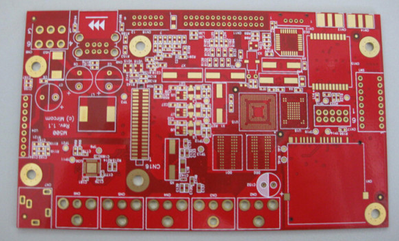
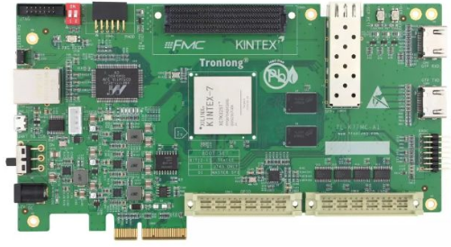
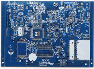
PCBA foundry material
Second, the advantages of PCBA foundry materials
1. As we all know, if companies want to streamline their production, they need a certain amount. Because the price of the MOQ of the product is very high, many small and medium-sized enterprises in the early start of the business if they use the PCB OEM model, it will often lead to a situation where they cannot make ends meet. With the development of the industry, a small PCB OEM model has emerged, allowing companies to conduct OEM business even if they only have a few sets of products. This greatly reduces the threshold for batches and enables more electronic products to be sold in After the design is completed, you can directly enter the foundry state, which greatly shortens the production cycle.
2. In the past, if you want to carry out PCBA OEM and materials business, the manufacturer's production batch is absolutely required. The production batch is not enough, and manufacturers have to pay a lot of additional management costs. However, with the development of the foundry industry, the foundry business for small enterprises has emerged. The current manufacturers do not have to worry about the previous problems at all. The manufacturer will only increase the appropriate cost based on the customer's list, instead of letting the customer directly bear the related management costs. This not only makes it easier for customers to accept, but also lowers the threshold for businesses to start.