1. PCB layout and assembly?
The first step in PCB design is to create a circuit diagram. Once the circuit diagram is completed, the PCB design and layout phase begins. Any circuit design is presented on paper or in circuit design software for easy understanding, but it is not necessary to meet such requirements for PCB design.
Although the connections on the circuit diagram and PCB design remain the same, the PCB layout is more powerful, designed to save space and follow different guidelines.
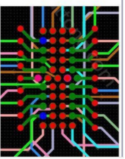
There are many different types of software that can help PCB design and layout. Software such as ADS or ARES can automatically create the PCB layout when the circuit diagram is given, but for more complex designs, the layout must be done manually to ensure optimization. Connections can be routed manually or depending on the PCB layout software,

they can be done manually.
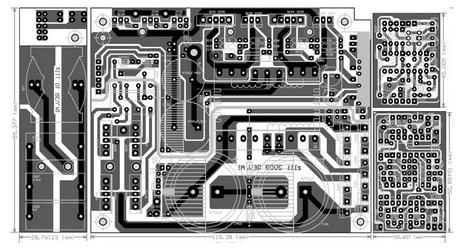
There are many different types of PCB layouts. The PCB layout of high frequency RF PCB is different from the traditional PCB layout of digital applications.
Therefore, in order to broadly classify, we have digital PCB layout, RF PCB layout, antenna layout and power supply layout. All different types of layouts have their own guidelines, such as the guidelines that need to be followed in RF. We must keep reflections in the transmission line to a minimum and ensure that no transmission lines are close to each other and affect the signal.
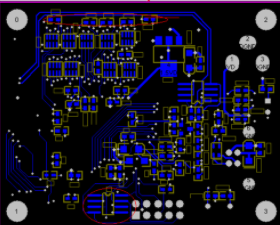
On the other hand, in the PCB layout of any digital application, we try to keep the copper tracks as close as possible to save space and reduce costs. For the same antenna layout, we must maximize any PCB layout and power supply, and heat dissipation is the main concern.
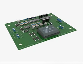
2. PCBA processing and SMT patch
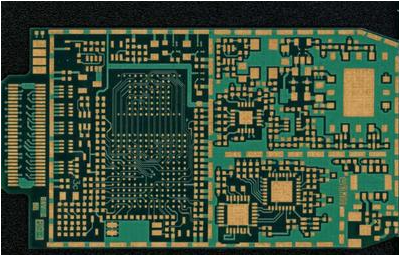
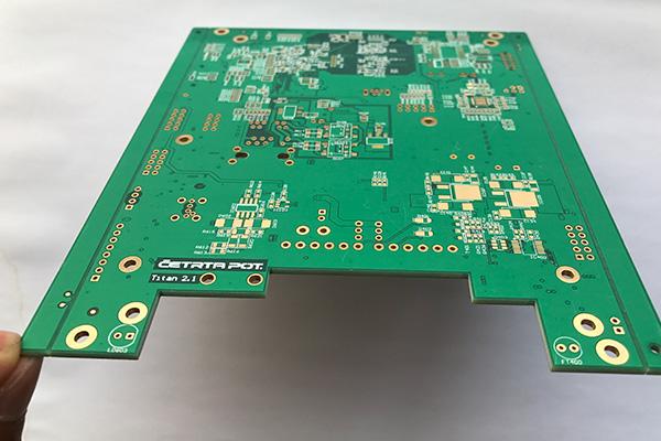
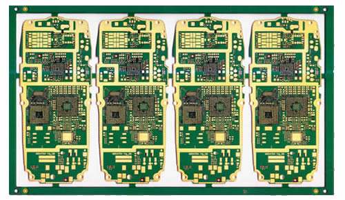
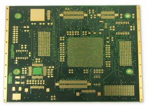
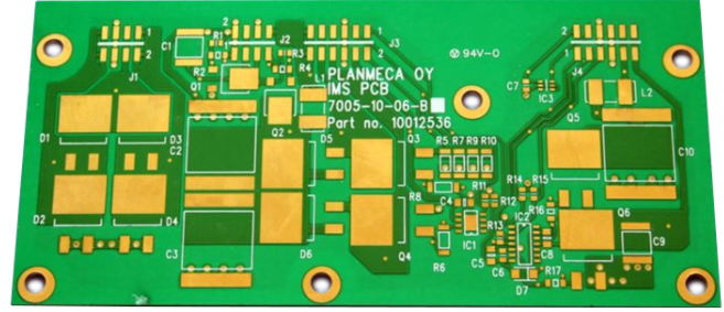
After the layout and design and layout are completed, the PCB assembly process begins. PCBs are created using any material of choice, the most common being FR4.
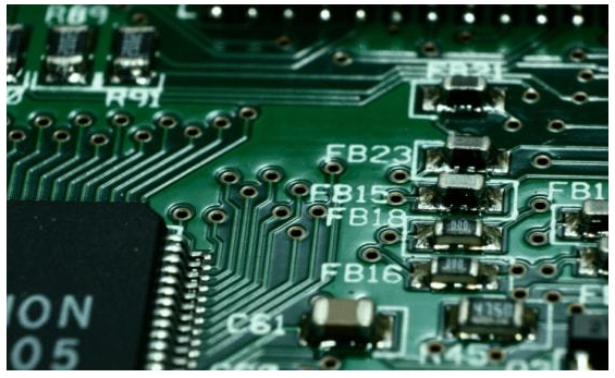
Various assembly processes (such as surface mount technology or through-hole structure) are used to mount electronic components on the PCB. The components used should also be compatible with the assembly process used.
The choice of PCBA The choice of PCB assembly depends on the complexity of the PCB design. Surface mount assembly technology is becoming more and more popular because it helps miniaturize any PCB.
For high-frequency RF printed circuit boards, surface mount components can reduce noise and reflections. For any printed circuit boards that do not apply these restrictions, we will choose printed circuit board components that can minimize costs.
The layout cost depends entirely on the complexity of the PCB design. For multi-layer high-speed designs, the layout cost is very high. This cost includes the tools required for this layout and the cost of hiring competent designers. The cost of assembly depends on the type and quality of the assembly process used. The cost of layout and design also depend on each other.
In addition, if the layout is not good, the assembly cost may be higher, and a better PCB layout can reduce assembly and production costs.