With the rapid development of electronic technology, the miniaturization, miniaturization of electronic components, BGA, and high-density chips with a pitch of 0.3mm~0.5mm are becoming more and more common, and the requirements for electronic welding technology are getting higher and higher. Although there are more sophisticated placement machines that can replace manual welding, there are too many factors that affect the quality of welding. This article introduces several points that need to be paid attention to when designing PCBs from the perspective of patch soldering. According to experience, if these requirements are not followed, it is likely to cause poor soldering quality, false soldering, and even damage to the soldering when reworking the PCB board. Disk or circuit board.
1. Factors affecting PCB soldering quality
From PCB design to the completion of all components soldering into a high-quality circuit board, it requires strict control of many links such as the PCB design engineer, as well as the soldering process and the level of soldering workers. The main factors are the following factors: PCB diagram, circuit board quality, device quality, device pin oxidation degree, solder paste quality, solder paste printing quality, precision of placement machine programming, placement machine placement Factors such as the quality of the package, the setting of the temperature profile of the reflow oven, and so on. The insurmountable link in the SMT soldering plant itself is the link of PCB drawing. Because circuit design people often do not solder circuit boards and therefore cannot obtain direct soldering experience, they do not know the various factors that affect soldering; while workers in SMT soldering plants do not understand PCB drawing board design, they just complete the production tasks without thinking, No ability to analyze the causes of poor welding. Since the talents in these two areas perform their duties, it is difficult to combine them organically.

2. Suggestions when drawing PCB diagrams
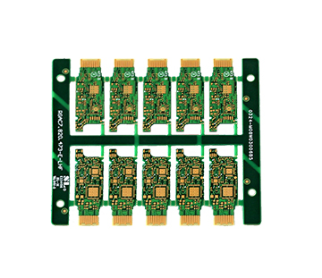
Next, I will give some suggestions to the design and wiring engineers who draw the PCB diagram in the process of PCB drawing, hoping to avoid all kinds of bad drawing methods that affect the welding quality during the drawing process. The introduction will be mainly in the form of pictures and texts.
1. Regarding positioning holes: Four holes (minimum aperture? 2.5mm) should be left on the four corners of the PCB for positioning the circuit board when printing solder paste. It is required that the centers of the X-axis or Y-axis directions are on the same axis.
2. About Mark point: used for placement machine positioning. Mark points should be marked on the PCB board, the specific location: on the diagonal of the board, it can be round or square pads, do not mix with the pads of other devices. If there are devices on both sides, both sides must be marked. When designing PCB, please pay attention to the following points:
a. The shape of the Mark point.
(Up and down symmetrical or left and right symmetrical)
b. The size of A is 2.0mm.
c. Within the range of 2.0mm from the outer edge of the Mark point, there should be no shape and color changes that may cause erroneous recognition. (Pad, solder paste)
d. The color of the Mark point should be different from the surrounding PCB color.
e. In order to ensure the recognition accuracy, copper or tin is plated on the surface of the Mark point to prevent surface reflection. For marks with only lines in the shape, the light spot cannot be recognized.
3. About leaving 5mm side: When drawing PCB, leave no less than 3mm side in the long side direction for the placement machine to transport the circuit board. Within this range, the placement machine cannot mount components. Do not place SMD devices within this range.
For the circuit board with components on both sides, it should be considered that the soldered side-to-side components will be wiped off during the second reflow. In severe cases, the pads will be wiped off and the circuit board will be destroyed.
Therefore, it is recommended not to place SMD devices within 5mm of the long side of the side with less chips (usually the Bottom side). If it is true that the area of the circuit board is limited, you can add process edges on the long side.
4. Do not directly pass holes on the pads: The defect of directly passing holes on the pads is that the solder paste melts and flows into the vias during over-reflow, causing the device pads to be short of tin and forming virtual soldering.
5. Regarding the polarity labeling of diodes and tantalum capacitors: The polarity labeling of diodes and tantalum capacitors should comply with the industry regulations, so as to prevent workers from soldering in the wrong direction based on experience.
6. Regarding silk screen and logo: please hide the device model. Especially circuit boards with high device density. Otherwise, dazzling affects finding the welding location.
The font size of silk-screened characters should not be too small to make it difficult to see clearly. The character placement position should be staggered through holes to avoid misreading.
7. Regarding IC pads should be extended: SOP, PLCC, QFP and other packaged ICs should be extended when drawing PCBs. The length of the pads on the PCB = IC foot length * 1.5 is appropriate, which is convenient for manual soldering with a soldering iron. The pins are fused with PCB pads and tin.
8. Regarding the width of the IC pad: SOP, PLCC, QFP and other packaged ICs, pay attention to the width of the pad when drawing the PCB, the width of the pad a on the PCB = the width of the IC foot (ie: the Nom. value in the datasheet) ), please do not increase the width, and ensure that b (that is, between the two pads) has enough width to avoid continuous welding.
9. Do not rotate any angle when placing the device: Since the placement machine cannot rotate at any angle, it can only rotate at 90°C, 180°C, 270°C, and 360°C. As shown in the following figure B rotated by 1°C, after the placement machine is mounted, the device pins and the pads on the circuit board will be staggered by an angle of 1°C, which affects the welding quality.
10. Problems that should be paid attention to when the adjacent pins are short-circuited: the short-circuit method in the figure a below is not conducive to workers to identify whether the pin should be connected, and it is not beautiful after welding. If you short-circuit as shown in Figure b and Figure c and add solder mask when drawing, the effect of soldering will be different: as long as each pin is not connected, the chip will not be short-circuited, and the appearance is also beautiful.
11. Regarding the problem of pads in the middle of the bottom of the chip: When drawing a chip with pads in the middle of the bottom of the chip, if you press the pad in the middle of the package drawing of the chip, it is easy to cause a short circuit. It is recommended to shrink the pad in the middle to increase the distance between it and the surrounding pin pads to reduce the chance of short circuit.
12. Two devices with higher thickness should not be arranged closely together: as shown in the figure below, the layout of the board will cause the placement machine to touch the previously pasted device when mounting the second device, and the machine will detect the danger and cause The machine automatically powers off.
13. About BGA: Due to the special BGA package, the pads are all under the chip, and the soldering effect cannot be seen outside. In order to facilitate the rework, it is recommended to make two positioning holes with Hole Size: 30mil on the PCB board to locate the stencil (used to scrape the solder paste) during rework. Reminder: The size of the positioning hole should not be too large or too small. It is advisable to make the needle not fall off, not shake, and a little tight when inserted, otherwise the positioning will be inaccurate.
14. Regarding the color of the PCB board: it is recommended not to make it red. Because the red circuit board is white under the red light source of the camera of the placement machine, it cannot be programmed and it is not convenient for the placement machine to solder.
15. Regarding the small devices under the large devices: some people like to arrange the small devices under the large devices on the same layer, for example: there is a resistor under the digital tube
16. Regarding the connection between the copper clad and the pad, which affects the soldering tin: Because the copper clad will absorb a lot of heat, it is difficult for the solder to melt sufficiently, thus forming a virtual solder.
Three, summary
Nowadays, there are more and more engineers who can use software to draw, route and design PCB, but once the design is completed, PCB welding efficiency can be improved.