The flexibility of FPC can be used for flexible design of connecting different circuits.
The size of 3C products is getting thinner and thinner, and the available internal structural space is limited. The design of the circuit board must be developed towards a 3D structure. Using the flexible combination of flexible boards and printed circuit boards, the design can adapt to different product configurations. Design, and at the same time use the advantages of the soft board to achieve the optimal state of the circuit design...
In today’s electronic product design, the evolution of PCB (Printed Circuit Board) responds to the trend of increasingly smaller terminal products. In response to the diversified product configuration design schemes, at this time, the overall design with flexible printed circuit board FPC (Flexible Print Circuit) and optimized flexible design for the product configuration have become an important design mode for consumer electronic products.
The circuit complexity and density that can be designed by FPC is inferior to that of PCB, but the flexible structure that can adapt to the structure has become the focus of electronic product design.
Aiming at the appearance design of consumer electronic products, FPC can do adaptive circuit design of any shape.
Today's electronic products are mostly soft? Hard board integration design requirements to achieve the goal of adapting to various product ID designs.

Rigid substrates such as PBC and HDI respond to the structural assembly requirements of different configurations, and the flexible design that can be done is limited, so they must be integrated with FPC soft boards for integrated design.
When designing multiple panels, we must first understand the characteristics of different panels and the current development trend. At the same time, the connection method between the panels, the use of connectors or the use of flexible and rigid boards, has different product characteristics and Use restrictions, these must be confirmed and evaluated before selecting design materials.
Understand the characteristics of different plates and integrate product design
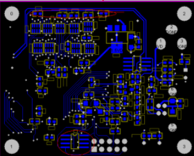
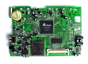
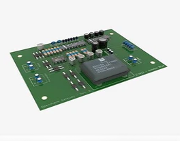
First of all, in terms of hard board, PCB printed circuit board can be said to be the largest type of carrier board currently used. In the early days, it was necessary to form an electronic circuit, in order to use wires to make circuit connections on the pins of electronic components. If it is an analog circuit with a simple layout, It may be okay to use wires for circuit connection, but if it is for multi-pin ICs, the circuit will become too complicated, and the design of the printed circuit board is a development solution derived to solve this design dilemma.
PCB printed circuit boards can be used to etch the copper foil on a carrier board to form electronic circuits through complete circuit planning and use of complex circuit copper wires between parts. PCB provides electronic components for installation and mutual The main substrate to be connected also has the effect of supporting and fixing electronic parts. Compared with the earlier structure of using wires, the electronic circuit can be more stable and have a longer life, and it can also reduce circuit misoperation or short circuit problems. PCB design Style has become an indispensable basic element.
The printed circuit board is basically a flat plate made of insulating material. It is equipped with pre-drilled positions for the installation and layout of the chip metal pins, and the electronic components are extended into the pre-drilled positions through the pins and then matched and soldered to make the components and the PCB carrier board. Combine. As for the preset pre-drilling of components, it can be used as component positioning. However, the design of pre-drilling requires manual plug-ins during mass production line manufacturing, which results in high manufacturing costs and manual plug-ins are also prone to manufacturing errors. It's not even easy to miniaturize the product design.
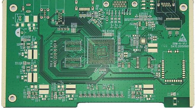
High-density and multi-layer design of PCB circuits in response to product miniaturization design trends
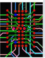
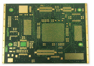
In response to the need to reduce the size of the carrier board, the printed circuit board also uses a double-sided, multi-layer structure to improve the circuit density. The size can be reduced by multiples. For the purpose of mass production, electronic parts are gradually changed to automatic feeding and soldering. The surface adhesion production process of the PCB, the original pre-drilling of the PCB is changed to the reserved soldering pad processing, so that the original plug-in program in the production is reduced to parts and materials to complete the assembly, which greatly increases the component arrangement density.
The configuration of electronic products is becoming more and more diversified, and there are many restrictions on the design of PCB. Because PCB is a hard insulating material, it has a certain degree of difficulty in shaping, especially in response to the curved and angled three-dimensional structure, which basically forms A large number of heavy industries and high-complex assembly will increase the cost of product development a lot, and it is also unfavorable to the miniature design of the product. Even if the cable and connector can be used for the integrated design of multiple PCBs, this will also increase the complexity and increase the production system. Defect rate problem.
In response to the PCB design requirements of different angles and non-flat circuits, flexible circuit boards of FPC flexible circuit boards have also been developed. Unlike the rigid multilayer PCB structure, the insulating substrate of FPC uses flexible insulating plastics. Using insulating plastic as the base material, and then attaching conductive lines to the base material, it becomes a flexible circuit type. PBC and FPC can be integrated to meet the circuit design requirements of different structures, and the application flexibility is more than that of the PCB-only solution. Good, and FPC has gradually become an indispensable key material for electronic product design like PCB.
FPC soft structure can improve the original PCB design restrictions
Flexible printed circuit boards and PCBs use copper foil as the conductive circuit design. The difference from rigid PCBs is that the printed circuit is arranged on a flexible substrate, and copper foil is used as the signal transmission medium for electronic components., Because FPC equipment can be continuously produced in large quantities, the circuit design can increase the wiring density, the weight of the FPC material is light, the thickness and volume of the material are quite small, and the occurrence of wiring errors can also be reduced, and it can even be adapted to different materials or structures Adaptable appearance design is currently quite common in electronic products such as digital cameras, mobile phones, and notebook computers.
Check the main structure of the soft board, which is mainly composed of rolled copper foil, insulating plastic substrate (PET or PI), adhesive (acrylic glue, epoxy resin), etc. The application material of the outer layer is mostly called Coverlay, which is used PET or PI coating protects the internal rolled copper foil structure to prevent the copper foil from being affected by external moisture and causing material degradation or oxidation. The key to FPC production is that precise coating procedures must be used to produce laminated copper foil structures. The environmental cleanliness requirements of the production process are high. Observing the cost structure of its materials, PI accounts for about 50% of the total cost, and the rest is The rolled copper foil is 35%, and the manufacturing cost is about 10%. A small part is the necessary processing cost of labor. It can be said that the biggest cost of FPC lies in the PI material.
Compared with the multi-layer type of PCB developed to HDI, FPC is not easy to develop multi-layer structure design due to the inherent limitations of manufacturing process and materials. Generally, 3L (Layer) is still the main part. For the connecting plates of boards and camera modules, the benefit of using FPC in large quantities is not as high as HDI. In most cases, the core circuit is the structure of the main component completed by the HDI multi-layer board structure, and the rest, such as peripheral modules, use soft boards. To integrate. FPC has many functions. It can be used as the data and circuit transmission intermediary between the hard boards of multiple PCB structures to achieve a flexible design solution that meets the product configuration. For the connection method of heterogeneous boards, you can choose a flexible board cable with a dedicated connector, You can also choose a design such as a flexible and hard board, so that the thickness of the terminal product can be reduced by reducing the height of the connector, and the use of more miniaturized terminal product size can be obtained.