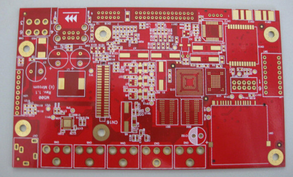
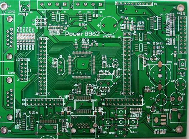
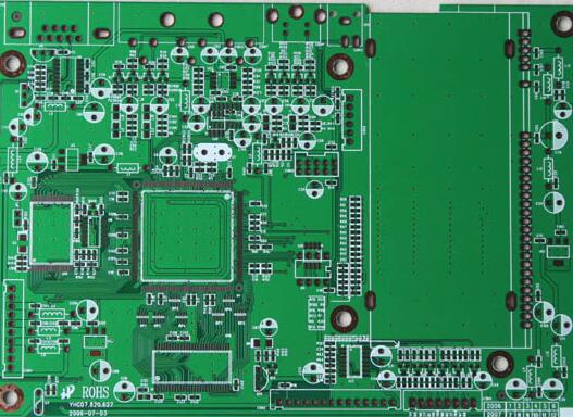
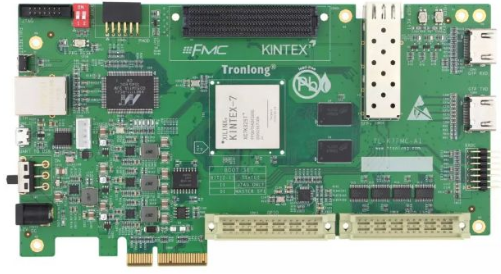
PCBA processing has appearance standards. The appearance of the board needs to be carefully checked during acceptance. Every small defect may cause the failure of PCBA processing.
1. Poor contact angle of the solder joint. The wetting angle between the fillet weld and the end joint of the land pattern is greater than 90°.
2. Upright: One end of the component leaves the pad and stands upright or obliquely upward.
3. PCBA processing short circuit: the solder between two or more solder joints that should not be connected is connected, or the solder of the solder joint is connected with adjacent wires.
4. Empty soldering: that is, the component leads and the PCB solder joints are not connected by soldering.
5. PCBA processing false welding: The component leads and the PCB solder joints seem to be connected, but they are not actually connected.
6. Cold welding: The solder paste at the solder joints is not completely melted or metal alloys are not formed.
7. Less tin (lack of tin consumption): The area or height of tin consumption between the component end and the PAD does not meet the requirements.
8. Too much tin (too much tin): The area or height of the component end and the PAD that eat tin exceeds the requirement.

9. The solder joints are black: the solder joints are black and dull.
10. Oxidation: The surface of components, circuits, PAD or solder joints has produced chemical reactions and colored oxides.
11. Displacement: The component deviates from the predetermined position in the horizontal (horizontal), vertical (vertical) or rotational direction in the plane of the pad.
12. PCBA processing polarity reversal (reverse): the direction of the component with polarity or the polarity of which does not meet the requirements of the document is reversed.
13. Floating height: There is a gap or height between the components and the PCB.
14. Wrong parts: the component specifications, models, parameters, shape and other requirements are not consistent with (BOM, samples, customer information, etc.).
15. Tin tip: The solder joints of the components are not smooth, and the tip is kept.
16. Multiple pieces: According to BOM and ECN or sample board, etc., there are multiple pieces where parts should not be installed or redundant parts on PCBA.
17. Missing parts: According to BOM and ECN or prototypes, etc., the parts that should be installed on the position or on the PCB but not parts are all missing parts.
18. Dislocation: The position of the component or component pin is moved to the position of other PAD or pin.
19. Open circuit: PCB circuit disconnection.
20. Side placement (side stand): The chip components with different width and height are placed on the side.
21. Reverse white: The two symmetrical surfaces with different components are interchangeable (such as: the surface with silk-screen logo and the surface without silk-screen logo are upside down), chip resistors are common.
22. PCBA processing tin beads: small tin spots between the feet of the components or outside the PAD.
23. Air bubbles: There are air bubbles inside solder joints, components or PCB.
24. Tinning (climbing tin): The height of the solder joints of the components exceeds the required height.
25. Tin crack: The solder joint is cracked.
26. Hole plug: PCB plug-in hole or via hole is blocked by solder or other.
27. Damage: cracks or cuts or damages in components, board bottom, board surface, copper foil, circuits, through holes, etc.
28. Blurred silk screen: The text or silk screen of the components or PCB is fuzzy or broken, which can not be recognized or blurred.
29. Dirty: The board surface is not clean, there are foreign objects or stains and other defects.
30. Scratches: PCBA processing or buttons and other scratches and exposed copper foil.
31. Deformation: The components or PCB body or corners are not on the same plane or bent.
32. Blistering (layered) PCB or components are layered with copper and platinum, and there is a gap.
33. Overflowing glue (too much glue) (excessive amount of red glue) or overflowing the required range.
34. Little glue (too little amount of red glue) or not up to the required range.
35. Pinhole (concave): PCB, PAD, solder joints, etc. have pinhole concavities.
36. Burr (over the peak): PCB board edge or burr exceeds the required range or length.
37. PCBA processing gold finger impurities: there are abnormalities such as pits, tin spots or solder mask on the surface of the gold finger plating.
38. Gold finger scratches: There are scratch marks or bare copper and platinum on the surface of the gold finger plating.