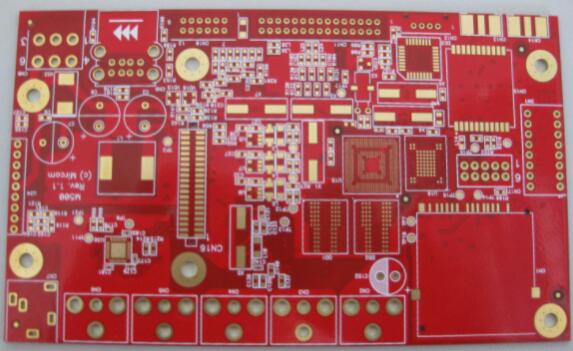
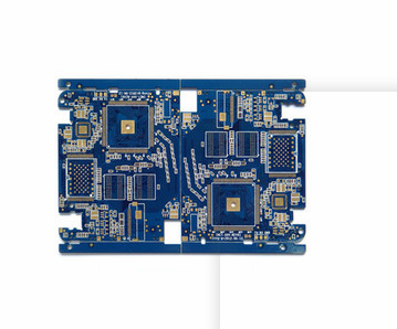
[OSP (Organic Solderability Preservative)] is a film that uses a chemical method to grow a layer of organic copper complex compound (complex compound) on the surface of copper. This organic film can protect the clean bare copper on the circuit board from rusting (vulcanization or oxidation) in contact with the air under normal storage conditions, and can be easily fluxed and diluted during the PCBA circuit board assembly process. The acid is quickly removed and the clean copper surface is exposed to form a weld with the molten solder.
This OSP is basically a transparent protective film. It is generally very difficult to detect its existence with the naked eye. Experts can see through refraction and reflection to see if there is a transparent film on the copper foil. There is not much difference between the OSP board and the ordinary bare copper board in appearance, which also makes it difficult for the board factory to check and measure the value.
If the organic copper protective agent (OSP) has a hole just on the copper surface, the copper surface will start to oxidize from the hole, which will affect the failure of SMT assembly. The thicker the organic copper protective agent, the greater the thickness of the copper foil. The better the protection, but relatively it also requires a stronger active flux to remove it for soldering, so the OSP film thickness is generally required to be between 0.2-0.5um.
Acid Cleaner (degreased):
The main purpose is to remove the copper surface oxides, fingerprints, grease and other pollution that may appear in the previous process to obtain a clean copper surface.
Micro-etch:

The main purpose of micro-etching is to remove serious oxides on the copper surface and produce a uniform and bright micro-rough copper surface, so that the subsequent OSP film can grow more finely and uniformly. Generally, the gloss and color of the copper surface after OSP film formation have a positive correlation with the selected micro-etching chemicals, because different chemicals will cause different roughness of the copper surface.
Acid Rinse:
The function of pickling is to thoroughly remove the residual material on the copper surface after microetching to ensure that the copper surface is clean.
OSP coating (organic flux protection treatment):
A layer of organic copper complex compound is grown on the copper surface to protect the copper surface from oxidation during storage. Generally, the OSP film thickness is required to be between 0.2-0.5um.
The factors that affect OSP film formation are:
▪ The pH value of OSP bath solution
▪ OSP bath concentration
▪ Total acidity of OSP bath
▪ Operating temperature
▪ Reaction time
Washing after OSP should strictly control its acid-base value above pH 2.1 to prevent over-acid washing from biting and dissolving the OSP film, resulting in insufficient thickness.
Dry:
In order to ensure the drying of the coating layer on the board surface and the holes, it is recommended to use hot air at 60-90°C for 30 seconds. (This temperature and time may have different requirements due to different OSP materials)
Advantages of OSP (Organic Solderability Preservative) surface treatment circuit board:
▪ The price is cheap.
▪ Good welding strength. The welding strength of OSP copper base is basically better than ENIG nickel base.
▪ Expired (three or six months) boards can also be resurfaced, but usually only once, depending on the board's condition.
OSP (Organic Solderability Preservative) surface treatment circuit board disadvantages:
▪ OSP is a transparent film, and its thickness is not easy to measure, so the thickness is not easy to control. The film thickness is too thin to find the effect of protecting the copper surface, and the film thickness is too thick to be welded.
▪ It is recommended to operate in an environment with open nitrogen during the secondary reflow, which can get a good welding effect.
▪ Insufficient shelf life. Generally speaking, after the OSP is completed in the PCB factory, its shelf life is up to six months, and some are only three months, depending on the ability of the board factory and the quality of the board, and some boards that have exceeded the shelf life can be returned The board factory washes off the old OSP on the PCB surface, and then re-applies a new layer of OSP. However, washing off the old OSP requires more corrosive chemicals, which will damage the copper surface more or less. Therefore, if the solder pad is too small, it will not be able to be processed. It is necessary to communicate with the board manufacturer whether the surface treatment can be done again.
▪ Easily affected by acid and humidity. When used in secondary reflow soldering (Reflow), it needs to be completed within a certain period of time. Generally, the effect of the second reflow soldering is relatively poor. It is generally required to use it up within 24 hours after opening the package (after reflowing). The shorter the time between the first reflow and the second reflow, the better. Generally, it is recommended to finish the second reflow within 8 hours or 12 hours.
▪ OSP is an insulating layer, so the test points on the board must be printed with solder paste to remove the original OSP layer in order to contact the needle points for electrical testing. Related reading: What is ICT (In-Circuit-Test)? What are the advantages and disadvantages?
▪ OSP board is a copper base. The benign IMC of Cu6Sn5 will be generated initially after soldering, but after time aging, it will gradually change to the inferior IMC of Cu3Sn, which will affect the reliability. The long-term reliability of OSP must be considered for products with service life.
Views on OSP surface treatment circuit boards:
Because of the low price of OSP, good weldability when fresh, good initial welding strength, poor weldability after a period of use, etc., OSP is very suitable for use in consumer products that are mass-produced at one time. If OSP can be used It is even more perfect that the IMC generated by the solder turns from benign Cu6Sn5 to strong Cu3Sn after a period of use (after the warranty period).
OSP is not suitable for a small number of diverse products, nor is it suitable for products with poor demand forecasts. If the inventory in the circuit board company often exceeds six months, it is really not recommended to use OSP. Surface treated board