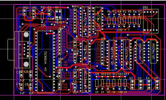
AD layout design output file
Now that you have completed the PCB design and routing, the user wants to generate output files to review, manufacture and assemble PCB boards. These files are usually used to provide board-level manufacturers, because there are a variety of different technologies and methods in PCB manufacturing, Altium Designer has the ability to generate many output files for various purposes.
These uses include:
Assembly output:
▪ Assembly drawing-display the position and origin information of the components on each side of the circuit board-representing the position and direction of the board.
▪ Grab, select and place files-used for component placement robots to place components on the circuit board-used by smart placement devices to intelligently place components.
File output:
▪ File output composite comprehensive drawing -- -Finished board assembly, including components and circuits.
▪ PCB three-dimensional printing, -- Adopt the three-dimensional view of the circuit board from the three-dimensional view.
▪ Schematic Schematic Print Print -- Designed-the settings used in the schematic diagram of the schematic drawing.

Production output:
▪ Draw a composite drilling diagram comprehensive presentation drawing --: Draw a composite drawing of the location and size of the drilling holes on the circuit board on the location and size of the demo board in a drawing.
▪ Demonstration drawing/guided drilling drawing/guide -- On multiple drawings: Demonstrate the location and size of the drilling plate in different drawings.
▪ Final drawing drawing: -- Combine all the production files into a single drawing output.
▪ Gerber file: -- Make the production information in Gerber format.
▪ NC Drill Files --- Create manufacturing information that can be used by CNC drilling machines.
▪ ODB++ --- Create manufacturing information in ODB++ database format.
▪ Power-Plane Prints --- Create multi-layer drawings of internal electric layer and electric layer division drawing department.
▪ Solder/Paste Mask Prints --- Create solder mask and paste mask drawings.
▪ Test Point Report --- Create output results of test points designed in different modes
Netlist output:
The network list describes the connection of components and components between logic on the PCB design, which is very helpful for transplanting to other electronic product designs.
Report output:
▪ Bill of Materials --- A list of parts and parts in different formats created for the needs of making boards.
▪ Component Cross Reference Report --- Create a list of components on the basis of the designed original diagram.
▪ Report Project Hierarchy --- Create a list of original documents on the project.
▪ Report Single Pin Nets --- Create a report to list any network with only one connection.
▪ Simple BOM --- Create text and a CSV (comma separated variable) file of the BOM.
Most of the output files are used for configuration, setting the output when needed. After you complete more designs, users will find that users often use the same or similar output files for each design.
Altium Designer provides a mechanism called Output Job Files, which uses an interface-Output Job Editor, which can be used to bundle various output files together and send them to various output media (direct printing, PDF and generated files).
Manual output file
In the final stage of the PCB design process, in order to better satisfy the production, we will explain in the guide how to generate Gerber and CNC drilling files, and BOM files. We no longer use Output Job Editor here, but use single-step menu commands-all output files can also be created directly from menu commands. Remember that the configuration output file is stored as part of the project.
Generate Gerber files
Each Gerber file is associated with a layer of the board --- device layer, top signal layer, bottom signal layer, solder masking layer and so on.
Generate Gerber files
It is advisable to consult the circuit board manufacturer to confirm their requirements before providing the output files for manufacturing.
Create an output file for the PCB in the tutorial:
Select File>>Fabrication Outputs>>Gerber Files. The setting dialog box is displayed.
Click the Layers tab, then the Plot Layers button, and select Used On. Click OK to accept the other default settings.
After the Gerber file is generated, it will be opened and displayed by the CAM editor. The Gerber file is stored in the Project Outputs folder, which is an automatically generated folder. Each file has an extension name that reflects its level, for example: multivibrator.gto is Gerber Top Overlay. These will be added to the Generated CAM Document folder in the Projects panel.
Similarly, select File>>Fabrication Outputs>>NC Drill Files command to open the NC Drill Setup dialog box to create through-hole data without connection.
Create a parts list
Create a bill of materials (BOM) for the PCB in the tutorial.
1. Select Reports>>Bill of Materials to display the Bill of Materials for PCB Document dialog box.
Parts list
2. Use this dialog box to build your own BOM. Enable the Show option in each column that the user wants to output to the report.
3. Select and drag the column title from the All Columns list to the Grouped Columns list, so that the components can be grouped by this data type in the BOM. For example, to group by package, select Footprint in All Columns and drag it to the list of Grouped Columns. The report will be classified accordingly.
4. Enable the Open Exported option, select CSV as the file format, and then click the Export button to create and immediately open the BOM file in your CSV viewer (such as Microsoft Excel). There are many BOM and other report types to choose from, which provides a high degree of flexibility. Close the dialog.
congratulate! You have completed the PCB design process.