The following describes how to solve the short circuit problem of the pin parts during wave soldering
Use "drag tin pad" or "steal tin solder pad" to solve the problem of solder bridge and tin short circuit
In the PCBA processing wave soldering (Wave Soldering) process, it is often heard to use "drag solder pad" or "steal solder pad" to solve the problem of solder bridge and solder short circuit. In fact, its English name is [solder thief pad]. Therefore, the correct Chinese name should be "Stealing Tin Soldering Pad", but everyone is screaming, now it seems to be called "Duo Tin" or "Stealing Tin". "Drag" is to drag the tin to another dummy pad, and "steal" is to steal the excess tin to another pad.
The main purpose of the "solder thief pad" setting is to prevent the solder feet of the components on the circuit board soldered by wave soldering from being dragged away from the solder joints when they slide out of the wave soldering surface. Later, because of the cohesive rebound of tin, the solder rebound buffer was designed to short-circuit the adjacent solder joints before it. This kind of solder rebound behavior usually occurs in the "advection wave" of wave soldering and rarely occurs in the "turbulent wave" ".
In addition, pin header (pin row) parts and parts with the entire row of solder pins parallel to the wave soldering direction are more prone to such short-circuit problems of solder springback.

Whether it is the "SO (Small Outline) package" SMD parts or the solder pins of the plug-in connector, as long as they pass through the wave soldering, there is a chance that this solder springback short-circuit problem will occur.
How to design the "solder thief pad" to improve the short circuit of wave soldering?
Generally, there are two ways to design "solder thief pad":
▪ Add a dummy pad. Add a dummy pad at the position behind the last pad in the downstream direction of wave soldering. The circuit of this pad must be empty (no signal) or connected to the circuit of the last pad. Dimensions It is the same size as the last pad.
▪ Extend the last pad size (Extended pad). Another rule is to extend the size of the last PCB solder pad by the size of the two solder pads directly back, that is, make the last solder pad three times the original length.
The purpose of this design is because the force of solder springback usually only reaches the previous solder joint, which is why when there is no stolen solder pad, the short circuit always occurs in the last two solder joints in the wave soldering direction. Since the short circuit cannot be avoided, Then turn the short circuit into a rationalization, so that even if it is short circuited, there will be no functional problems.
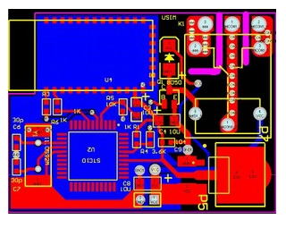
Stealing the solder pad
As for the advantages and disadvantages of these two designs, the difference is not very big. If you insist, "adding a fake solder pad" may be easier to cause disputes between the production line and the quality control, because the quality control staff always think that there is a short circuit. Defects, or all of them should be short-circuited or open-circuited. The same batch of production has some short-circuits and some open-circuits, indicating that the quality is unstable.
"Extending the last solder pad" is more unfavorable for repairs, because the tin area becomes larger, and more heat needs to be given during repairs, which can easily damage the solder pads.
In terms of production quality alone, Shenzhen Honglijie recommends "Extend the last solder pad" because the larger solder area can effectively absorb the rebound force of the solder, instead of allowing the solder to bounce back to the previous solder joint without any control. When the quality of the production line is completed, the maintenance is relatively reduced, and the quality control is also satisfied. Everyone is happy!
Can I use a tray oven carrier to replace the "solder thief pad"?
Furnace tray and tin sheet
This is a very feasible and can be tried, in fact, some people have designed it like this.
If the process itself requires a carrier for wave soldering, then a "Solder thief tool" can be designed on the wave soldering carrier to replace the soldering pad on the PCB. However, its location must be similar or the same as the design of the solder pad on the PCB, and the size must be in accordance with the "extend the last solder pad" instead of "add a fake solder pad". It is practically recommended to use this The tin stealing piece is made a little longer than the soldering pad on the PCB, but remember not to be too close to the solder joints in front to avoid bridging the solder joints between the stealing tin piece and the PCB. Once the bridge is required It is troublesome when removing the PCB from the carrier.
In addition, the tin stealing piece on this vehicle must meet the following requirements:
▪ The stolen tin piece must be of a material that can eat tin.
▪ PCB material should be considered reusable. Because the vehicle needs to be reused many times, the stolen tin piece can also be reused many times. You can consider using steel, then nickel plating and then tin plating. The main consideration is that it must be able to eat tin repeatedly. The copper sheet is too soft and will deform after repeated use, and lead-free wave soldering will bite copper.
▪ The thickness should also be paid attention to. Too thin is easy to deform, too thick will block the flow of solder, about 1.0mm should be about the same.
▪ Must be fixed on the vehicle and cannot be moved.
▪ Consider the issue of replacement. Stealing tin will inevitably be damaged after use for a long time. Generally, it is recommended to use screws to fix them, which can be replaced. Of course, the screws must choose not to eat tin.
▪ No sharp angles and sharp points are allowed. Because stealing tin will contact the PCB board, sharp corners and sharp points will have the opportunity to scratch the board.