The research and development of PCBA module mainly involves two aspects: hardware design and software design; the so-called planning and then move, before the module design. Need to consider from these aspects, program selection, schematic and layout design, PCB board and PCBA processing and proofing, index debugging and parameter testing; among them, the program selection is the most important.
1. Scheme selection
The core is to meet the functions, easy to supply and produce, and price matching.
1. Demand analysis
Functional considerations: the networking mode used by wifi, one-to-one or one-to-many. One-to-one for terminal products, one-to-many for gateways and routing.
In terms of transmission rate, it is divided into flow type and control type. If the module is used in the control of smart home appliances, select a control type chip, such as ESP8266; if it is used in a product such as a router, it is necessary to select a flow type chip, such as 7620 of MTK.
In terms of functional interfaces, PCBA module developers consider more possibilities for the number of chip interfaces, functional support, etc., such as GPIO function port, SPI flash expansion port, I2C interface; in fact, this is well understood, such as RTL8710, the Internet of Things WiFi chip, it has more than twenty GPIOs, supports more input and output devices, or more external connections or controls.
The same consideration of interface functions cannot be ignored. For example, some interfaces of this chip can automatically reduce the power consumption to the lowest state when it is not working, and can automatically wake up from sleep mode when it enters the working state, which can greatly Reduce the power consumption of the product. In addition, in terms of application functions, PCBA module developers can choose transparent or non-transparent chip solutions according to their needs.

2. Analysis of advantages and disadvantages
In addition to analyzing the market demand for chip solutions, PCBA module developers also need to consider the cost and stability of the chip, as well as the original factory and supply channels. Even if a good product is excellent in all aspects, but the price is out of the market, no one dares to choose. Of course, you can't just look at the price. As the saying goes, it makes sense that cheap is not good. If the difference between the advantages of the two chip solutions is obvious, the chip solution with the dominant advantage will not stop everyone from choosing even if the price is a little higher. When it comes to the stability of the chip solution, this is particularly critical. If it is a chip that has high power consumption and can easily cause heat and cause crashes, how do you let product developers and consumers choose? Of course, heat generation and PCBA heat dissipation may be one of the many factors that cause instability. For example, the chip manufacturer's inadequate optimization of the software code will also cause the above problems.
2. Schematic design
After PCBA module developers choose the chip solution, they must carry out PCBA module development and design. The first task of PCBA module development and design is to design the schematic diagram.
1. Stability: The developer needs to design a PCBA schematic diagram with high stability according to the specification requirements based on the chip information provided by the chip manufacturer.
2. Cost advantage: There are many design schemes for the schematic diagram, but the consideration of PCBA processing cost cannot be ignored. For example, two-layer PCB design and four-layer PCB design can be used. Four-layer PCB is also better, but the price is more expensive. Of course, this is only one aspect of cost considerations.
3. Compatibility design: The electromagnetic compatibility design consideration in the schematic design is to consider that the PCBA module can still work in a coordinated and effective manner in a variety of electromagnetic environments. The purpose is to ensure that the PCBA module can suppress all kinds of external interference, so that the PCBA module can work normally in a specific electromagnetic environment, and at the same time can reduce the electromagnetic interference of the PCBA module itself to other electronic devices. EMC design considerations involve the stability and performance of the entire module.
4. The difficulty of PCBA mass production: The schematic design should also consider whether it is convenient for PCBA processing in the future. Good PCBA processing means that PCBA processing costs are less. If the designed schematic diagram results in a low yield rate of actual PCBA processing, it will also increase the cost.
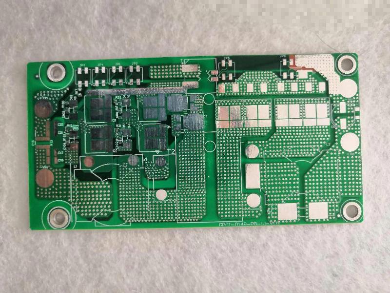
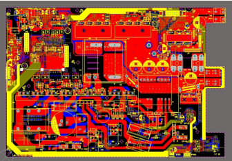
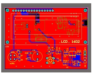
Three, draw the PCB board
The schematic design of the upper part, together with the drawing of the PCB board, is collectively referred to as PCB Layout. The two are complementary. The design of the schematic diagram is to be reflected on the PCB board. The schematic diagram should also be considered when drawing the PCB board, and there is more to be considered when drawing the PCB board. For example, radio frequency considerations, stability considerations, structural considerations, and even the aesthetics of the board need to be considered when drawing a PCB board. Because from the drawing method of the board, we can see whether the PCBA module manufacturer is professional or not.
Of course, according to the PCB selection involved in the PCB Layout design scheme, various material conditions such as resistance, capacitor type and quantity will be reflected in the BOM (Bill of Material) bill of materials. The same PCB, SMT patch production, etc. are also shown in this form. To determine the material.
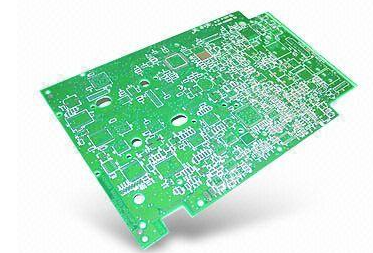
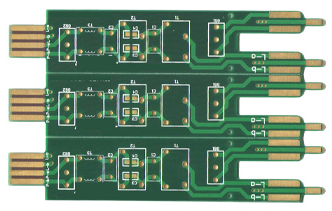
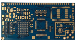
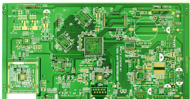
Four, PCB proofing
PCB (Printed Circuit Board) is called "printed circuit board", made of epoxy glass resin material, with different signal layers, and chip and other chip components are attached to the PCB. PCB processing manufacturer selection: For PCB proofing, if PCBA module manufacturers look for external manufacturers, they usually need to consider whether these manufacturers have module PCB proofing experience, whether the manufacturer’s equipment meets the needs, whether the manufacturer’s management is good, and so on.
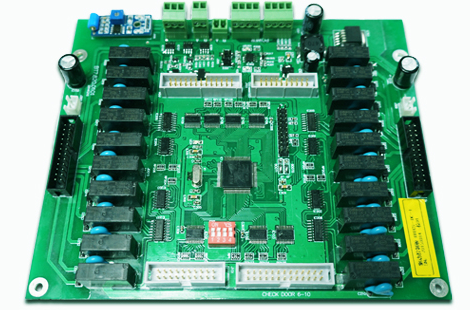
Five, PCBA proofing
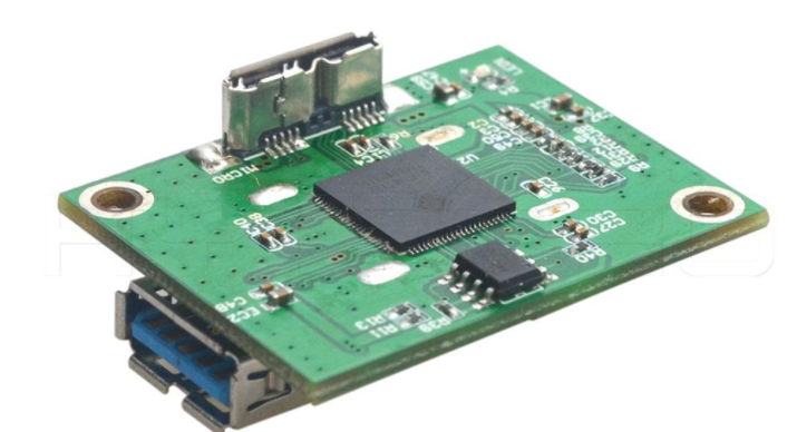
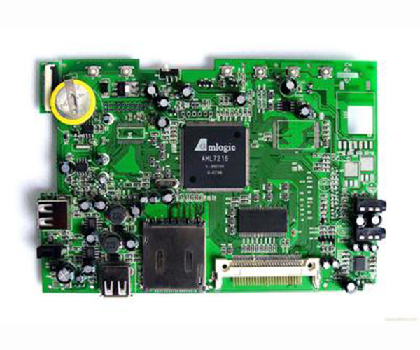
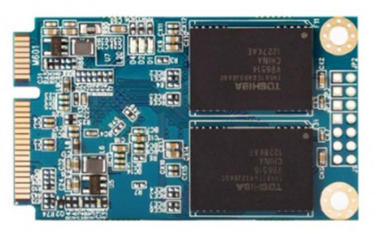
PCBA (Printed Cirruit Board + Assembly,) means that the empty PCB board goes through SMT and then goes through the entire process of DIP plug-in, referred to as PCBA, which may be understood as a finished circuit board.
Six, debugging
The debugging of PCBA module mainly lies in hardware circuit debugging and software debugging. Generally, the radio frequency part of Wi-Fi products consists of several parts, and the blue dashed box is regarded as the power amplifier part. The radio transceiver (Radio Transceiver) is generally one of the core components of a design. In addition to its close relationship with the radio frequency circuit, it is generally related to the CPU. Here we only pay attention to some of its content related to the radio frequency circuit. When sending a signal, the transceiver itself will directly output a low-power weak RF signal, send it to the Power Amplifier (PA) for power amplification, and then radiate it through the antenna (Antenna) through the Transmit/Receive Switch. space.
When receiving a signal, the antenna will sense the electromagnetic signal in the space, and then send it to the Low Noise Amplifier (LNA) for amplification after passing through the switch, so that the amplified signal can be directly sent to the transceiver for processing and decoding. Tune. PCBA hardware debugging mainly involves the debugging of radio frequency circuits and functional circuits. Radio frequency debugging includes two major aspects: transmission and reception. Transmission includes transmission power and phase error adjustment. Reception includes sensitivity and reception level. The functional circuit debugging is more related to the circuit debugging of a specific hardware function module.
Seven, test
The so-called electronic circuit test is a repeated process of a series of measurement, judgment, adjustment, and re-measurement for the purpose of achieving the circuit design index.
1. Functional test: According to the features, operation descriptions and user schemes supported by the PCBA module, test the features and operational behaviors of the module to determine whether it meets the design requirements.
2. Performance test: It mainly involves testing each functional circuit of the module, as well as other parameters such as signal transmission distance.
3. Stability test: Test the stability of the actual transmission rate, actual power consumption, throughput, and wireless connection of the involved module.
4. Aging test: It is a test for the life of the PCBA module and the best effect during use. Because the system is in working condition for a long time, load operation of each device during its work, as long as the stable performance of the equipment can be ensured under these conditions, the service life of the working module under normal environment will be longer.
5. Certification test: some products must be certified by the certification body designated by the relevant country