In the field of PCB manufacturing business, PCB companies need to always maintain an efficient multi-variety rapid delivery capability, aiming to build China’s strongest PCB prototype and small and medium batch manufacturing plants, combining high-quality lean production management, R&D and manufacturing capabilities, and the company’s continuous construction Leading advantages such as PCB core technology help Chinese companies with independent intellectual property rights to continuously accelerate technological innovation and development.
After the wiring of the PCB circuit board is completed, the circuit board should be checked for design rules to ensure that the circuit board meets the design requirements and all networks have been correctly connected. Commonly used inspection items in design rule inspection are as follows:
1. Whether the distance between the line and the line, the line and the component pad, the line and the via hole, the component pad and the via hole, the via hole and the via hole is reasonable, and whether it meets the production requirements.

2. Whether the width of the power line and the ground line is appropriate, whether the power supply and the ground line are tightly coupled, and whether there is a place to widen the ground line in the middle.
3. Whether the best measures have been taken for the key signal lines, such as the shortest length, the protection line, the input line and the output line are clearly separated.
4. Whether there are separate ground wires for the analog circuit and digital circuit part.
5. Whether the graphics (such as icons, annotations) added to the PCB board will cause signal short circuit.
6. Whether to modify some unsatisfactory lines.
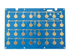
7. Whether there is a process line on the PCB, whether the solder mask meets the requirements of the production process, whether the solder mask size is appropriate, and whether the character logo is pressed on the device pad.
8. Whether the outer frame edge of the power ground layer in the multilayer board is reduced, such as the copper foil of the power ground layer is exposed, which may cause a short circuit.
Design rule inspection results can be divided into two types: one is Report (report) output, which generates inspection result reports; the other is On Line inspection, which is to inspect the electrical rules and wiring rules of the circuit board during the wiring process.
This article mainly introduces PCB design rules, including electrical rules, wiring, layout rules, high-speed circuit design rules, signal integrity and other rules. Through the study of this chapter, I have a detailed understanding of the design rules of the circuit board, and lay the foundation for the production of high-efficiency PCB.
The future goal of PCB company is to establish the most efficient and strongest rapid manufacturing platform in the field of PCB prototypes and multiple varieties of small and medium-sized batches; to provide many technological innovation enterprises, including small and micro enterprises, with rapid proofing and mass production manufacturing services of advanced electronic products; and It will gradually build an open technical service platform, build a team of experienced PCB technical consultants and experts, and form a comprehensive solution capability for common core technologies in the field of electronic hardware design, combined with supporting multi-variety rapid placement service capabilities, to provide customers with a personalized one Station type hardware outsourcing services.