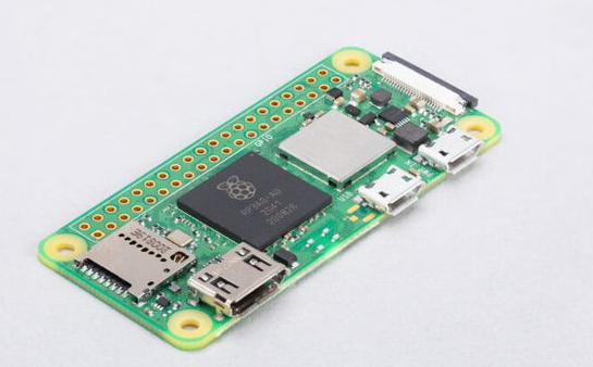
Each curved line on the circuit board represents a different signal. If the lines on the circuit board are designed to be straight lines, it is easy for the signals to interfere with each other, making our electronic equipment unable to work normally. If the signal of our mobile phone is interfered, it is likely that there is a problem with the circuit board, and such a mobile phone can almost be scrapped.
When the CO_2 laser drills directly, the copper thickness is controlled in the range of 8≤9μm, and the fluctuation of the blind aperture is the smallest. The laser parameters for direct erosion of blind holes by CO_2 laser can be preliminarily determined..
It can be seen from the application of the frontal cross test that when ablating the dielectric layer, the type of the dielectric layer substrate must be determined, and then the amount of pulses must be determined. As a fine-tuning of the laser parameters, the laser parameters of a blind hole with a good quality 0.13mm aperture thickness-to-diameter ratio of 1:1 can be obtained: under a MASK of 2.2mm.
The first step is a 14.μ pulse width of 17mj.
The second step is to switch to 5 US pulse width 7 times under the same calibration value. During the blind hole filling and electroplating process, the quality of the filled hole is affected by factors such as the blind hole of the plating solution.

Through the experimental analysis of related influencing factors, it can be seen that the copper acid content is higher than the blind hole filling quality of the plating solution. During the filling process, the current density has a great influence on the filling of blind holes. Consider the copper growth rate inside the blind via and on the surface of the board. The concentrations of copper sulfate and sulfuric acid are 220ml/L and 80ml/L, respectively, and the filling current is 2.0a/m~2. The plating time is 85 minutes, and the jet flow rate is 280L/min.
The type of PCB single-sided board is divided.
94HB single-sided paper substrate 94V0 single-sided paper substrate 22F single-sided half glass fiber board CEM-1 single-sided half glass fiber board CEM-3 single-sided half glass fiber board FR-4 single-sided glass fiber board. Single-sided aluminum substrate, etc.
PCB single-sided processing.
Baking board-cutting-grinding board-drilling-sinking copper-board electricity-outer layer etching-electricity-silk screen-exposure-characters-spray tin (lead). According to customer needs, molding-V cutting-cleaning-electrical testing-final inspection-packaging.
The design of the multi-layer high frequency board is based on the electromagnetic interference control of cost saving and bending strength. The selection and stacking design of high frequency mixed pressure materials are various. The high frequency RO4350B/RO4450B and FR4 material combination mixed pressure are used.
The test results show that the superposition design of the high-frequency hybrid board is based on one or more factors of cost saving, bending strength, and electromagnetic interference control. In this case, it is necessary to use a high-frequency semi-cured film and FR-4 substrate with a relatively low fluidity dielectric surface. During the compression process, the adhesion control of the product faces greater risks. Professional HDI circuit board..
The experimental results show that the key technologies such as the compression parameter control of the compression slow pressure material designed by the FR-4A material plate edge spherical bonded baffle block are used. Achieve good adhesion between mixed pressure materials.
The production process of the blind hole plate is as follows.
A Mechanical deep drilling.
The traditional multilayer board process uses a drilling machine to set the drilling depth, but this method has several problems.
Only one drill at a time is very low.
The level of drilling rig B is strictly required. The depth setting of each diamond should be consistent, otherwise it is difficult to control the depth of each hole.
The difficulty of electroplating in the hole is particularly higher than the depth of electroplating in the hole. It is almost impossible for HDI PCB manufacturers to do a good job of plating inside holes.
The limitations of the above processes make this method gradually not used.
BB suppresses Sequentialamination again and again.
Take the eight-layer board as an example, press one by one, and make blind buried holes at the same time. First of all, the four inner layers can be combined with a general double-sided skin thread and PTH. Six-layer double-sided board, upper and lower double-sided board, four-layer board, and then four-layered into a four-layer board, and then completely through the hole. It is not common that this method is more expensive than other methods.
C layer-adding method (non-machine drilling method).
At present, this method is the most popular in the world, and it is no less than the manufacturing experience of some large PCB factories in China.