PCB board design can be output to printer or output light drawing file. The printer can print the PCB in layers, which is convenient for designers and reviewers to check; the gerber file is handed over to the board manufacturer to produce the printed board. The output of the gerber file is very important. It is related to the success or failure of this design. The following will focus on the matters needing attention when outputting the gerber file.
a. The layers that need to be output are wiring layers (including top layer, bottom layer, middle wiring layer), power layer (including VCC layer and GND layer), silk screen layer (including top silk screen, bottom silk screen), solder mask layer (including top solder mask) And bottom solder mask), and also generate a drilling file (NC Drill).

b. If the power layer is set to Split/Mixed, then select Routing in the Document item of the Add document window, and before outputting the gerber file each time, you must use Pour Manager's Plane Connect to pour copper on the PCB diagram; if it is set to CAM Plane, select Plane. When setting the Layer item, add Layer25, and select Pads and Viasc in Layer.25. In the device setup window (press Device Setup), change the value of Aperture to l99.
D. When setting the Layer of each layer, select the Board outline.
E. When setting the Layer of the silk screen layer, do not select Part Type, select the Outline, Text, and Line of the top layer (bottom layer) and the silk screen layer.
F. When setting the layer of the solder mask, selecting vias means that no solder mask is added to the vias, and not selecting vias means solder masking, which depends on the specific situation.
G. When generating drilling files, use the default settings of PowerPCB and do not make any changes.
H. After all the gerber files have been output, open and print them with CAM350, and check them by the designer and reviewer according to the PCB checklist"
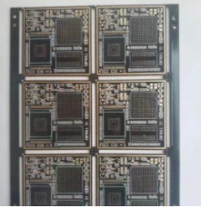
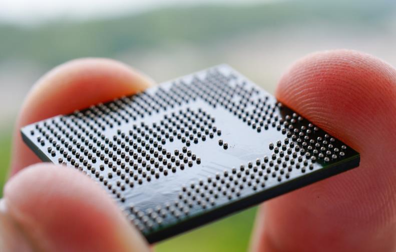
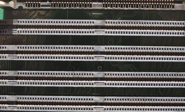
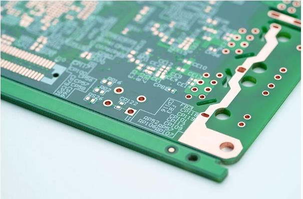
Via is one of the important components of multilayer PCB. The cost of drilling usually accounts for 30% to 40% of the PCB manufacturing cost. Simply put, every hole on the PCB can be called a via. From the point of view of function, vias can be divided into two categories: one is used for electrical connections between layers; the other is used for fixing or positioning devices. In terms of process, these vias are generally divided into three categories, namely blind vias, buried vias and through vias. Blind vias are located on the top and bottom surfaces of the printed circuit board and have a certain depth. They are used to connect the surface line and the underlying inner line. The depth of the hole usually does not exceed a certain ratio (aperture). Buried hole refers to the connection hole located in the inner layer of the printed circuit board, which does not extend to the surface of the circuit board. The above-mentioned two types of holes are located in the inner layer of the circuit board, and are completed by a through-hole forming process before lamination, and several inner layers may be overlapped during the formation of the via. The third type is called a through hole, which penetrates the entire circuit board and can be used for internal interconnection or as a component mounting positioning hole. Because the through hole is easier to implement in the process and the cost is lower, most of the printed circuit boards use it instead of the other two types of through holes. The following via holes, unless otherwise specified, are considered as via holes.
From a design point of view, a via is mainly composed of two parts: one is the drill hole in the middle, and the other is the pad area around the drill. The size of these two parts determines the size of the via. . Obviously, in high-speed, high-density PCB design, designers always hope that the smaller the via hole is, the better, so that more wiring space can be left on the board. In addition, the smaller the via hole, the greater its own parasitic capacitance. Small, more suitable for high-speed circuits. However, the reduction of hole size also brings about an increase in cost, and the size of vias cannot be reduced indefinitely. It is limited by process technologies such as drilling and electroplating: the smaller the hole, the more time it takes to drill. Longer, the easier it is to deviate from the center position; and when the depth of the hole exceeds 6 times the diameter of the drilled hole, it is impossible to ensure that the hole wall can be uniformly plated with copper. For example, the thickness (through hole depth) of a normal 6-layer PCB board is about 50Mil, so the minimum drilling diameter that PCB manufacturers can provide can only reach 8Mil.