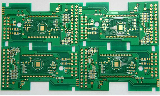
1. FPC circuit board drilling and surface treatment
FPC circuit board hole metallization, the hole metallization of flexible circuit board is basically the same as that of rigid circuit board.
In recent years, there has been a direct electroplating process that replaces electroless plating and adopts the technology of forming a carbon conductive layer. The hole metallization of flexible printed circuit board also introduces this technology.
Due to its softness, flexible printed boards need special fixing fixtures. The fixtures can not only fix the flexible printed boards, but also must be stable in the plating solution. Otherwise, the thickness of the copper plating will be uneven, which will also cause disconnection during the etching process. And the important reason for bridging. In order to obtain a uniform copper plating layer, the flexible printed board must be tightened in the fixture, and work must be done on the position and shape of the electrode.
Hole metallization outsourcing processing should be avoided as much as possible to factories without flexible printed board boring experience. If there is no dedicated electroplating line for flexible printed boards, the quality of boring cannot be guaranteed.
Copper foil surface cleaning-FPC manufacturing process

In order to improve the adhesion of the resist mask, the surface of the copper foil must be cleaned before coating the resist mask. Even such a simple process requires special attention for flexible printed boards.
Generally, there are chemical cleaning process and mechanical polishing process for cleaning. For the manufacture of precision graphics, most occasions are combined with two kinds of clear flow processes for surface treatment. Mechanical polishing uses the method of polishing. If the polishing material is too hard, it will damage the copper foil, and if it is too soft, it will be insufficiently polished. Generally, nylon brushes are used, and the length and hardness of the brushes must be carefully studied. Use two brushing rollers, placed on the conveyor belt, the rotation direction is opposite to the belt conveying direction, but if the pressure of the brushing rollers is too large at this time, the substrate will be stretched under great tension, which will cause dimensional changes One of the important reasons.
If the surface of the copper foil is not clean, the adhesion to the resist mask will be poor, which will reduce the pass rate of the etching process. Recently, due to the improvement of the quality of copper foil boards, the surface cleaning process can also be omitted in the case of single-sided circuits. However, surface cleaning is an indispensable process for precision patterns below 100μm.
Two, FPC circuit board film selection
FPC circuit board resist coating and filming process. Now, the resist coating method is divided into the following three methods according to the precision and output of the circuit pattern: screen printing method, dry film/photographic method, liquid resist Etching agent photosensitive method.
The anti-corrosion ink uses the screen printing method to directly print the circuit pattern on the surface of the copper foil. This is the most commonly used technology and is suitable for mass production with low cost. The precision of the formed circuit pattern can reach line width/spacing 0.2~O. 3mm, but not suitable for more sophisticated graphics. With the miniaturization, this method is gradually unable to adapt. Compared with the dry film method described below, a certain technical operator is required, and the operator must undergo years of training, which is a disadvantageous factor.
Dry film method can produce 70-80μm line width patterns as long as the equipment and conditions are complete. At present, most of the precision patterns below 0.3mm can be formed by dry film method to form resist circuit patterns. Using dry film, its thickness is 15-25μm, conditions permit, batch level can produce 30-40μm line width graphics.
When choosing a dry film, it must be determined according to the compatibility with the copper foil board and process and through experiments. Even if the experimental level has a good resolution ability, it does not necessarily have a high pass rate when used in mass production. The flexible printed board is thin and easy to bend. If a harder dry film is selected, it will be brittle and have poor follow-up properties, so cracks or peeling will also occur, which will reduce the pass rate of etching.
The dry film is in roll form, and the production equipment and operation are relatively simple. The dry film is composed of a three-layer structure such as a thin polyester protective film, a photoresist film and a thicker polyester release film. Before attaching the film, first peel off the release film (also called diaphragm), then press it on the surface of the copper foil with a hot roller, and then tear off the protective film (also called carrier film or cover film) before developing. Generally, there are guiding and positioning holes on both sides of the flexible printed board, and the dry film can be slightly narrower than the flexible copper foil board to be pasted. The automatic filming device for rigid printed boards is not suitable for the filming of flexible printed boards, and some design changes must be made. Due to the high linear speed of dry film lamination compared with other processes, many factories do not use automatic lamination, but use manual lamination.
After sticking the dry film, in order to make it stable, it should be placed for 15-20 minutes before exposure.