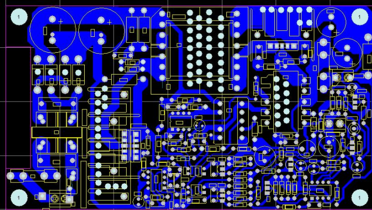
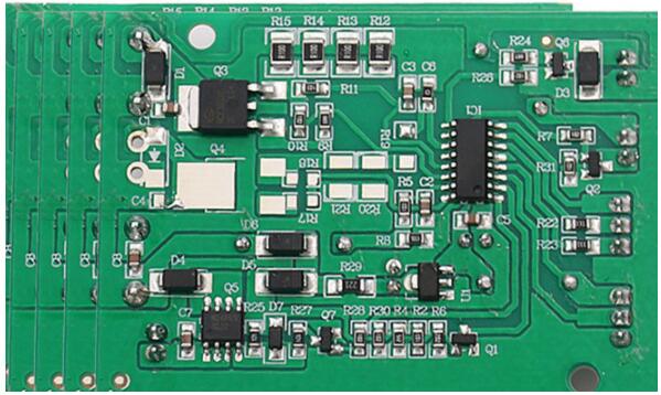
Common errors in PCB circuit boards
(1) It is reported that NODE is not found when loading the network. The components used in the PCB library have inconsistent packages with pin numbers. For example, a triode: the pin numbers in sch are e, b, and c, while those in PCB are 1, 2, and 3.
(2) It is always impossible to print onto one page when printing
a. It is not at the origin when creating the PCB library; b. The component has been moved and rotated many times, and there are hidden characters outside the boundary of the PCB board. Choose to show all hidden characters, shrink the PCB, and then move the characters to the boundary.
(3) The DRC reporting network is divided into several parts:
Indicates that this network is not connected. Look at the report file and use CONNECTED COPPER to find it.
If you make a more complicated design, try not to use automatic wiring.
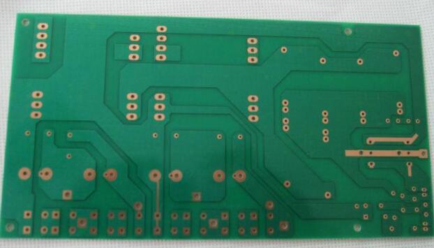
Common mistakes in the manufacturing process of PCB circuit boards (1) Overlap of pads a. Causes heavy holes. When drilling, multiple holes are drilled in one place, which leads to broken drills and hole damage. b. In the multi-layer board, there are both connection plates and isolation plates at the same position, and the board is shown as? isolation and connection errors.
(2) Irregular use of graphics layer a. Violation of conventional design, such as component surface design in the Bottom layer, welding surface design in the TOP layer, causing misunderstandings. b. There are a lot of design rubbish on each layer, such as broken lines, useless borders, labels, etc.

(3) Unreasonable characters a. The characters cover SMD soldering tabs, which brings inconvenience to PCB on-off detection and component soldering.
b. The characters are too small, which makes screen printing difficult. If the characters are too large, they will overlap each other and be difficult to distinguish. The font is generally >40mil.
(4) Single-sided pad setting aperture a. Single-sided pad is generally not drilled, and its aperture should be designed to be zero, otherwise the coordinates of the hole will appear at this position when drilling data is generated. Special instructions should be given for drilling. b. If a single-sided pad needs to be drilled, but the aperture is not designed, the software treats this pad as an SMT pad when outputting electrical and ground data, and the inner layer will lose the isolation disk.
(5) Draw PCB pads with filler blocks
Although it can pass the DRC inspection, the solder mask data cannot be directly generated during processing, and the pad is covered with solder mask and cannot be soldered.
(6) The electrical ground layer is designed with both a heat sink and a signal line. The positive and negative images are designed together, and errors occur.
(7) Large area grid spacing is too small
The grid line spacing is less than 0.3mm. During the PCB manufacturing process, the pattern transfer process will cause film breakage after development, which will increase the processing difficulty.
(8) The graphics are too close to the frame
At least 0.2mm or more spacing should be ensured (V-cut 0.35mm or more), otherwise the copper foil will warp and the solder resist will fall off during the exterior processing, which will affect the appearance quality (including the inner copper skin of the multilayer board).
(9) The outline frame design is not clear
Many layers are designed with frames and do not overlap, which makes it difficult for PCB manufacturers to determine which line to use. The standard frame should be designed on the mechanical layer or the BOARD layer, and the internal hollowed-out parts should be clear.
(10) Uneven graphic design
When the pattern is electroplated, the current distribution is uneven, which affects the uniformity of the coating, and even causes warpage.
(11) Short shaped hole
The length/width of the special-shaped hole should be> 2:1, and the width should be> 1.0 mm, otherwise the CNC drilling machine cannot process it.
(12) Milling profile positioning hole is not designed
If possible, design at least two positioning holes with a diameter of> 1.5mm in the PCB board.
(13) The aperture is not clearly marked
a. The aperture marking should be marked in metric system as far as possible, and in increments of 0.05. b. Combine the apertures that may be combined into a reservoir area as much as possible. c. Whether the tolerances of metallized holes and special holes (such as crimp holes) are clearly marked.
(14) Unreasonable wiring in the inner layer of the multilayer board
a. The heat dissipation pad is placed on the isolation tape, and it is easy to fail to connect after drilling. b. There are gaps in the design of the isolation belt, which is easy to misunderstand. c. The isolation band design is too narrow to accurately judge the network