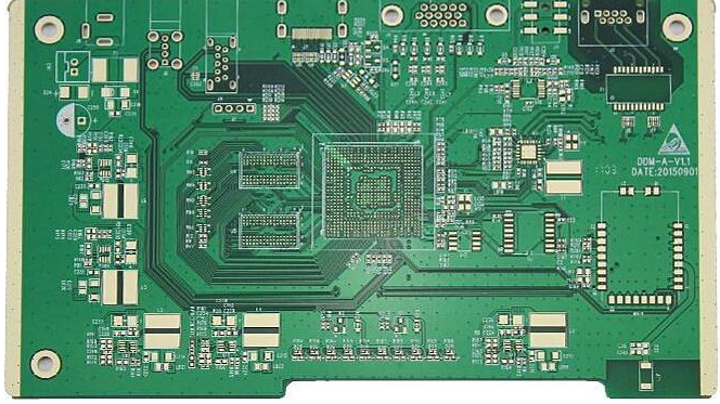
1. In the PCB design layout, all components should be arranged on the same side of the circuit board. Only when the top components are too dense, can some devices with limited height and low heat generation, such as chip resistors, chip capacitors, Chip ICs, etc. are placed on the lower layer.
2. Under the premise of ensuring the electrical performance, the components should be placed on the grid and arranged parallel or perpendicular to each other in order to be neat and beautiful. Under normal circumstances, the components are not allowed to overlap; the arrangement of the components should be compact, and the components should be arranged on the entire layout. The distribution is uniform and dense.
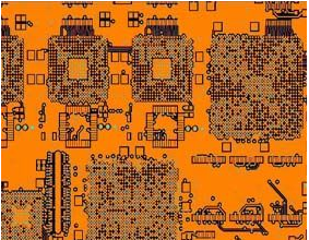
3. The minimum distance between adjacent land patterns of different components on the circuit board should be above 1mm.
4. The distance from the edge of the circuit board is generally not less than 2MM. The best shape of the circuit board is rectangular, with an aspect ratio of 3:2 or 4:3. When the size of the circuit board is larger than 200MM by 150MM, consider what the circuit board can withstand Mechanical strength.
In the layout design of the PCB, the units of the circuit board should be analyzed, and the layout design should be based on the starting function. When laying out all the components of the circuit, the following principles should be met:
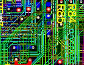
1. Arrange the position of each functional circuit unit according to the circuit flow, so that the layout is convenient for signal circulation, and the signal is kept in the same direction as possible.
2. Take the core components of each functional unit as the center and lay out around him. The components should be uniformly, integrally and compactly arranged on the PCB to minimize and shorten the leads and connections between the components.
How to control the quality of PCB circuit boards
1. The concept of PCB circuit board proofing

What is PCB proofing? It means that after the electronic engineer has designed the circuit board of the electronic product, he placed an order to the PCB circuit board factory for testing without making money for mass production. The production quantity of PCB circuit board proofing generally has no specific boundaries. Before the product design of the electronic engineer is confirmed and tested, it is called PCB circuit board proofing.
2. How to control the quality of PCB circuit board?
The general PCB circuit board proofing that has not been ordered in batches before the test is qualified is slightly higher, the delivery time is faster, and the quality is better. PCB circuit manufacturers are particularly important in terms of independent testing. Today, Shenchuang Electronics will share with friends how we control the quality of Shenchuang Electronics.
Stage 1 Quality is checked
Generally, those who make electronic products know that PCB circuit boards need to go through a series of processes such as drilling and sinking copper during production, and they have set up quality inspection positions in various processes, and they are responsible for inspecting each circuit board produced by the process. And why is there a shortage of our deep-creation electronics?
Phase 2 Quality is manufactured
After so many years of continuous development of electronic products, after the products are manufactured, they will be checked and accepted. The timeliness and economics are not up to the expected targets. The quality control is born. It is expected that the quality can be controlled in the process of PCB manufacturing. And the production department also needs self-inspection.
Stage 3 Quality is used to it