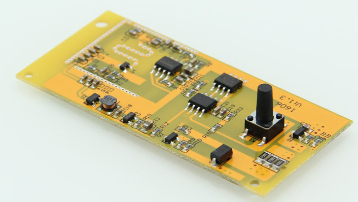
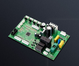
The following is a talk about circuit board design experience: multi-layer PCB circuit board design grounding experience, about grounding treatment:
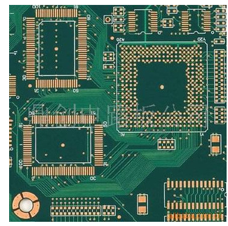
According to the rule of thumb, four-layer boards are usually used in high-density and high-frequency applications, which are more than 20DB better than two-layer boards in terms of EMC. Under the condition of a four-layer board, a complete ground plane and a complete power plane can often be used. Under this condition, only the ground wires of the circuits divided into several groups are connected to the ground plane, and the working noise is particularly special. deal with.
There are many ways to connect the ground wire of each circuit to the ground plane, including: single-point and multi-point grounding
1. Single-point grounding: The ground wires of all circuits are connected to the same point on the ground plane, which is divided into series single-point grounding and parallel single-point grounding.

2. Multi-point grounding: The ground wires of all circuits are grounded nearby, and the ground wires are short and suitable for high-frequency grounding.
3. Mixed grounding: mix single-point grounding and multi-point grounding.
Between low frequency, low power and the same power layer, single-point grounding is the most appropriate, and it is usually used in analog circuits; here, the star connection is generally used to reduce the influence of possible series impedance. High-frequency digital circuits need to be grounded in parallel, where it is generally easier to deal with through ground holes; generally, all modules will use two grounding methods, and a mixed grounding method is used to complete the circuit grounding and the ground plane. connect.
If you do not choose to use the entire plane as a common ground wire, for example, when the module itself has two ground wires, you need to divide the ground plane, which often interacts with the power plane. Pay attention to the following principles:
(1) Align the planes to avoid the overlap between the unrelated power plane and the ground plane, otherwise it will cause all the ground planes to fail and interfere with each other;
(2) In the case of high frequency, there will be coupling between layers through the parasitic capacitance of the circuit board;
(3) The signal lines between the ground planes (such as the digital ground plane and the analog ground plane) are connected by a ground bridge, and the closest return path is configured through the nearest through hole.
(4) Avoid running high-frequency traces such as clock lines near the isolated ground plane, which may cause unnecessary radiation.
(5) The area of the loop formed by the signal line and its loop is as small as possible, which is also called the minimum loop rule; the smaller the loop area, the less external radiation, and the less interference from the outside world. When dividing the ground plane and signal routing, consider the distribution of the ground plane and important signal traces to prevent problems caused by slotting in the ground plane.
Circuit board design experience talk: multi-layer PCB circuit board design grounding experience, about the connection method between grounds
1. Common wiring connection of circuit boards between grounds: Using this method can ensure reliable low-impedance conduction between the middle and two ground wires, but it is limited to the connection between the medium and low frequency signal circuit grounds.
2. PCB large resistance connection between the ground: the characteristic of the large resistance is that once the voltage difference between the two ends of the resistance occurs, a very weak conduction current will be generated. After the charge on the ground line is discharged, the voltage difference between the two ends is finally zero. .
3. PCB capacitor connection between ground: The characteristics of the capacitor are DC cut-off and AC conduction, which are used in floating systems.
4. PCB magnetic bead connection between ground: magnetic bead is equivalent to a resistance that changes with frequency, and it shows resistance characteristics. It is used between the ground and the ground of the weak signal with fast and small current fluctuations.
5. PCB inductance connection between grounds: Inductance has the characteristics of restraining the change of circuit state, can cut peaks and fill valleys, and is usually used between two grounds with large current fluctuations.
6. PCB small resistance connection between grounds: a small resistance adds a damping, which prevents the overshoot of the rapid change of the ground current; when the current changes, the rising edge of the inrush current is slowed down