The following is a summary of PCB multilayer board design principles for readers to refer to when designing, and can also be used as a basis for reference when checking after the design is completed.
1. PCB component library requirements
(1) The package of the components used on the PCB must be correct, including the size and size of the component pins, the spacing of the pins, the number of the pins, the size and direction of the frame, etc.
(2) The positive and negative poles or pin numbers of polar components (electrolytic capacitors, diodes, triodes, etc.) should be marked in the PCB component library and on the PCB board.
(3) The pin numbers of the components in the PCB library should be consistent with the pin numbers of the schematic components. For example, the pin numbers in the diode PCB library components are inconsistent with the pin numbers in the schematic library in the previous chapter. problem.
(4) For components that require heat sinks, the size of the heat sink should be taken into account when drawing the component package, and the components and heat sink can be drawn together into an overall package form.

(5) The inner diameter of the pin of the component and the pad should be matched, and the inner diameter of the pad should be slightly larger than the pin size of the component to facilitate installation.
2. PCB component layout requirements
(1) The components are arranged uniformly, and the components of the same functional module should be arranged as close as possible.
(2) The components that use the same type of power supply and ground network are arranged together as much as possible, which is beneficial to complete the electrical connection between each other through the inner electrical layer.
(3) The interface components should be placed aside, and the interface type should be indicated with a character string, and the direction of the wiring should usually be away from the circuit board.
(4) Power conversion components (such as transformers, DC/DC converters, three-terminal regulator tubes, etc.) should have enough space for heat dissipation.
(5) The pins or reference points of the components should be placed on the grid point, which is conducive to wiring and aesthetics.
(6) The filter capacitor can be placed on the back of the chip, close to the power and ground pins of the chip.
(7) The first pin of the component or the sign indicating the direction should be marked on the PCB and cannot be covered by the component.
(8) The label of the component should be close to the component frame, uniform in size, neat in direction, not overlapping with pads and vias, and cannot be placed in the area covered after the component is installed.
3. PCB wiring requirements
(1) Power supplies of different voltage levels should be isolated, and power supply wires should not cross.
(2) The wiring adopts 45° corners or circular arc corners, and no sharp corners are allowed.
(3) The PCB trace is directly connected to the center of the pad, and the width of the wire connected to the pad is not allowed to exceed the outer diameter of the pad.
(4) The line width of the high-frequency signal line is not less than 20mil, and the external ground wire is used to surround it, which is isolated from other ground wires.
(5) Do not wire the bottom of the interference source (DC/DC converter, crystal oscillator, transformer, etc.) to avoid interference.
(6) Thicken the power line and ground line as much as possible, and the width of the power line should not be less than 50mil if space permits.
(7) The signal line width of low voltage and low current is 9~30mil, and should be as thick as possible if space permits.
(8) The spacing between signal lines should be greater than 10 mils, and the spacing between power lines should be greater than 20 mils.
(9) The line width of high-current signal lines should be greater than 40 mils, and the spacing should be greater than 30 mils.
(10) The minimum size of the via hole is preferably 40 mil outer diameter and 28 mil inner diameter. When connecting with wires between the top layer and the bottom layer, pads are preferred.
(11) It is not allowed to arrange signal lines on the inner electric layer.
(12) The width of the interval between different areas of the inner electrical layer is not less than 40 mils.
(13) When drawing the boundary, try not to let the boundary line pass through the pads of the area to be connected to.
(14) Laying copper on the top and bottom layers, it is recommended to set the line width value greater than the grid width to completely cover the vacant space and leave no dead copper. At the same time, keep a distance of more than 30mil (0.762mm) from other lines (copper can be used in the Set the safety distance before, and change it back to the original safety distance after the copper coating is completed).
(15) Teardrop the pad after wiring.
(16) The metal shell device and the external grounding of the module.
(17) Place the pads for mounting and soldering.
(18) The DRC check is correct.
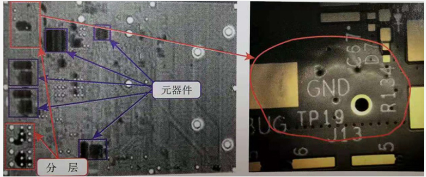
4. PCB delamination requirements
(1) The power plane should be close to the ground plane, tightly coupled with the ground plane, and arranged below the ground plane.
(2) The signal layer should be adjacent to the inner electrical layer, not directly adjacent to other signal layers.
(3) Isolate digital circuits and analog circuits. If conditions permit, arrange the analog signal lines and digital signal lines in layers, and adopt shielding measures; if they need to be arranged on the same signal layer, they need to use isolation bands and ground lines to reduce interference; power supplies for analog circuits and digital circuits And the ground should be isolated from each other and cannot be mixed.
(4) The high-frequency circuit has a large external interference, and it is best to arrange it separately, and use the intermediate signal layer directly adjacent to the inner electric layer above and below for transmission, so as to use the copper film of the inner electric layer to reduce external interference.