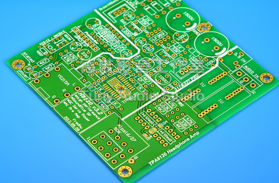
With the vigorous development of surface mount technology, the future trend of PCB printed circuit boards will inevitably move toward high-density packaging of fine lines, small holes, and multiple layers. However, the copper plating process for manufacturing such high-level circuit boards will also face some Technical bottleneck. In recent years, with the rapid development of the semiconductor and computer industries, the production of printed circuit boards has become increasingly complex. Circuit board complex program pointer = PCB circuit board layer number * number of wires between two solder joints / two solder joint spacing (inches) *Example of wire width (mil):
A 16-layer board with a solder joint pitch of 0.1 inches and a wire width of 5 mils. There are three wires between the two solder joints, and its complexity index is 96. Since the 1980s, the popularity of surface mounting technology has driven the circuit board industry to a higher level. The advancement of multi-layer boards has led to a rapid increase in complex indicators, from about 20 in traditional circuit boards to the current 100 or higher. In the process of such updates and product evolution, of course, some technical bottlenecks are unavoidable. Taking the copper plating process as an example, the author tries to explore its basic principles and seek corresponding strategies from three aspects: macro, micro, and microstructure.

The macro aspect refers to the board surface of the PCB circuit board. Usually the size of a large board is about 24"*18". It is not easy to make the center and edge coating thickness uniform. According to Faraday's law of electrolysis, the coating The thickness is proportional to the applied current. Assuming that the density of the coating is a certain value, the thickness distribution of the coating is the distribution of the cathode current. Many factors affecting the current distribution include the resistance in the solution, the polarization of the electrode, the geometry of the plating, and the yin and yang. The distance between the poles, the magnitude of the applied current, the mass transfer rate, etc., we will discuss the effects in the following sections respectively. When the current distribution on the electrode does not produce polarization or other interference factors, it is called the primary current distribution. In the geometry of the plating tank, when a certain voltage is applied to the two electrodes, there is also a certain voltage at each point in the plating bath, which is between the voltages of the two electrodes. Because the metal electrode is very conductive, we can assume that the electrode The voltage at every point on the surface is equal, and some imaginary planes with equal potential can also be found in the plating bath. Generally speaking, when approaching the position of the electrode, the equipotential plane is very similar to the shape of the electrode, but its shape varies. As the distance from the electrode gradually increases and changes, the distribution of the equipotential plane of the PCB has a higher current density where the equipotential distribution is denser, and vice versa. It is known from the electric field theory that the equipotential plane and its The planes of stress are perpendicular to each other, and the electrode itself belongs to the equipotential plane, so a certain point of the current flowing into or out of the electrode must be perpendicular to the plane where the point is located. The relationship between the equipotential plane of the PCB board and the distribution of the current flow. If the PCB, etc. The replacement of the potential plane by a certain whole conductor or the replacement of the stress plane on the equipotential surface with an insulator will not affect its electric field. On the contrary, if the equipotential surface is cut by any substitute, the entire electric field will be subjected to the same degree The current distribution will also change. Take one as an example. Using A and BB as electrodes and A and C as electrodes will get the same current distribution. The main reason is that the BB plane coincides with the equipotential plane. Therefore, it will not affect the electric field. Assuming that A and C in Figure 1 are slightly moved to make them deviate from the center position, the distribution of equipotential lines will be very different from the original, because the change of the electrode position affects the electric field so that The current distribution has also changed.