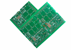
According to the characteristics of the circuit board material and the wide range of applications, in order to more effectively save volume and achieve a certain degree of accuracy, the three-dimensional characteristics and thin thickness are better applied to digital products, mobile phones and notebook computers. Recommended instruments suitable for circuit board (FPC) testing include MUMA200 all-aluminum alloy optical image measuring instrument, three-axis automatic optical image measuring machine VMC250S, VMC four-axis automatic optical image measuring instrument, VMS series optical image measuring instrument and so on.
Test Methods
Needle bed method
In this method, a probe with a spring is connected to each detection point on the circuit board. The spring makes each probe have a pressure of 100-200g to ensure good contact between each detection point. Such probes are arranged together and are called a "bed of needles". Under the control of the detection software, the detection points and detection signals can be programmed. Figure 14-3 is a typical needle bed tester structure, and the inspector can get the information of all the test points. In fact, only the probes of the test points that need to be tested are installed. Although it is possible to use the bed-of-needle test method to test on both sides of the circuit board at the same time, when designing the circuit board, all inspection points should be made on the soldering surface of the circuit board.

The needle bed tester is expensive and difficult to repair. According to the specific application of the needle, the probes in different arrangements are selected.
A basic general-purpose grid processor consists of a drilled board with 100, 75, or 50 mils center-to-pin spacing. The pins act as probes and use electrical connectors or nodes on the circuit board to make direct mechanical connections. If the pads on the circuit board match the test grid, the polyester film perforated in accordance with the specification will be placed between the grid and the circuit board to facilitate the design of specific probes. Continuity detection is achieved by accessing the end points of the grid (which have been defined as the x-y coordinates of the pad). Since every network on the circuit board is tested for continuity. In this way, an independent test is completed. However, the proximity of the probe limits the effectiveness of the bed-of-needle test method.
Observation
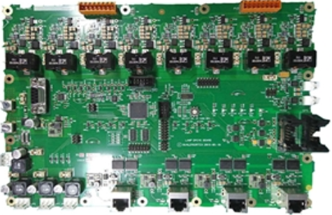
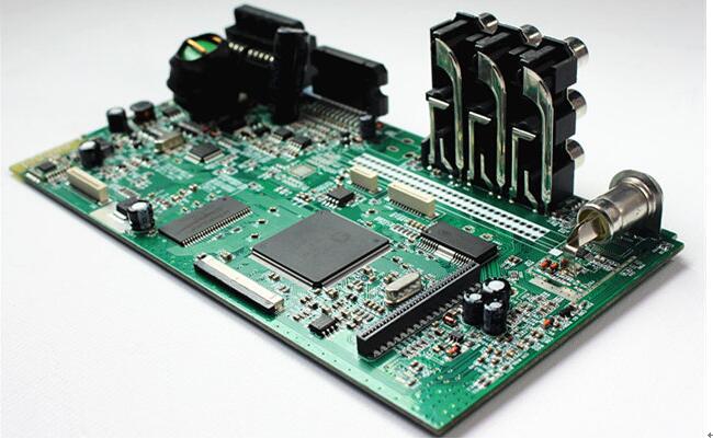
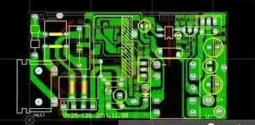
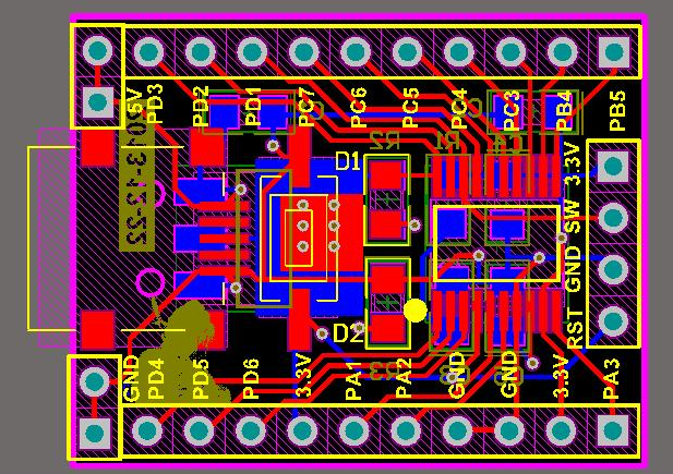
The circuit board is small in size and complex in structure, so the observation of the circuit board must also use professional observation instruments. Generally, we use a portable video microscope to observe the structure of the circuit board. Through the video microscope camera, you can clearly see the very intuitive microstructure of the circuit board from the microscope. In this way, it is easier for us to design and test the circuit board. The portable video microscopes currently used in the PCB factory site, the portable video microscopes MSA200 and VT101, are more convenient than traditional microscopes because they can realize "observation, detection and multi-person discussion at any time"!
Flying probe test
The flying probe tester does not rely on the pin pattern installed on the fixture or bracket. Based on this system, two or more probes are mounted on a tiny magnetic head that can move freely on the x-y plane, and the test points are directly controlled by CADI Gerber data. The dual probes can move within a distance of 4 mils from each other. The probes can move independently, and there is no real limit to how close they are to each other. The tester with two arms that can move back and forth is based on the measurement of capacitance. The circuit board is pressed tightly and placed on the insulating layer on a metal plate as the other metal plate of the capacitor. If there is a short circuit between the lines, the capacitance will be larger than at a certain point. If there is an open circuit, the capacitance will become smaller.
Testing speed is an important criterion for selecting a tester. The bed of needle tester can accurately test thousands of test points at a time, while the flying probe tester can only test two or four test points at a time. In addition, the needle bed tester may only cost 20-305 for a single-sided test, depending on the complexity of the board, while the flying probe tester requires Ih or more time to complete the same evaluation. Shipley (1991) explained that even if manufacturers of high-volume printed circuit boards consider moving flying probe testing techniques to be slow, this method is still a good choice for manufacturers of complex circuit boards with lower yields.
For bare board testing, there are dedicated test instruments (Lea, 1990). A more cost-optimized method is to use a general-purpose instrument. Although this type of instrument is initially more expensive than a dedicated instrument, its initial high cost will be offset by the reduction in individual configuration costs. For general grids, the standard grid for boards with pin components and surface mount equipment is 2.5mm. At this time, the test pad should be greater than or equal to 1.3mm. For Imm grids, the test pad is designed to be larger than 0.7mm. If the grid is small, the test needle is small, brittle, and easily damaged. Therefore, it is best to choose a grid larger than 2.5mm. Crum (1994b) stated that the combination of a universal tester (standard grid tester) and a flying probe tester can make the inspection of high-density circuit boards both accurate and economical. Another method he suggested is to use a conductive rubber tester, which can be used to detect points that deviate from the grid. However, the height of the pads that are leveled by hot air is different, which will hinder the connection of the test points.
The following three levels of testing are usually carried out:
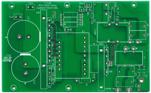
1) Bare board inspection;
2) Online testing;
3) Functional testing.
The universal type of tester can be used to test a class of styles and types of PCB circuit boards, and it can also be used for special applications.