When PCBA welding is processed, there are usually many requirements for PCBA board, and the board must meet the requirements to accept welding processing. So why does the welding process need so many requirements for the board? It turns out that during the processing of PCBA, there will be a lot of special processes, and the application of special processes immediately brings requirements to the PCB board. If there are problems with the PCB board, it will increase the difficulty of the PCBA soldering process, which may eventually be Lead to welding defects, unqualified boards, etc. Therefore, in order to ensure the smooth completion of the processing of the special process and to facilitate the PCBA welding process, the PCB board must meet the manufacturability requirements in terms of size, pad distance, etc., then today I will take you to see the PCBA welding process The requirements of the PCB board.
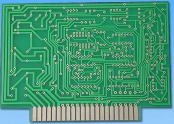
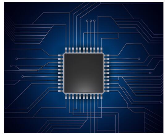
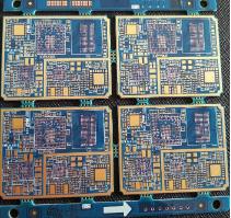
PCBA board

1. PCB size
The width of the PCB (including the edge of the board) should be greater than 50mm and less than 460mm, and the length of the PCB (including the edge of the board) should be greater than 50mm. If the size is too small, it needs to be made into a jigsaw.
2. PCB board edge width
Board edge width: >5mm, panel spacing: <8mm, distance between pad and board edge: >5mm
3. PCB bending
Upward bending degree: <1.2mm, downward bending degree: <0.5mm, PCB distortion: maximum deformation height ÷ diagonal length <0.25
4. PCB board mark point
Mark shape: standard circle, square, triangle;
Mark size: 0.8~1.5mm;
Mark material: gold-plated, tin-plated, copper and platinum;
Mark's surface requirements: the surface is flat, smooth, non-oxidized, and free of dirt;
Mark's surrounding requirements: there should be no green oil or other obstacles within 1mm, which is obviously different from the Mark's color;
Mark position: 3mm above the edge of the board, and there should be no Mark-like vias, test points, etc. within 5mm around the board.
5. PCB pads
There are no through holes on the pads of SMD components. If there is a through hole, the solder paste will flow into the hole, resulting in less tin in the device, or the tin flowing to the other side, causing the board surface to be uneven and the solder paste cannot be printed.
When conducting PCB design and production, it is necessary to understand some knowledge of PCBA welding process, so as to make the product suitable for production. Understanding the requirements of the processing plant first can make the subsequent manufacturing process more smooth and avoid unnecessary troubles. This is the requirement of PCBA welding process for PCB board.
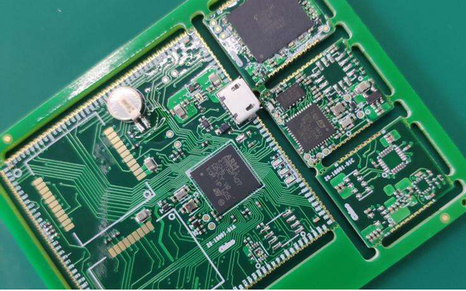
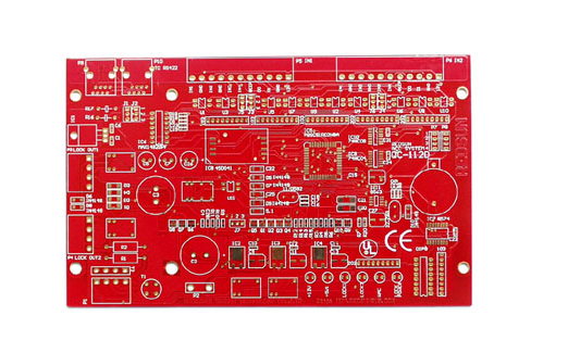
SMT proofing process
Printed circuit board is an important electronic component, it is also a support for electronic components, and it is also a provider of electronic component circuit connection. Today we mainly introduce its processing process!
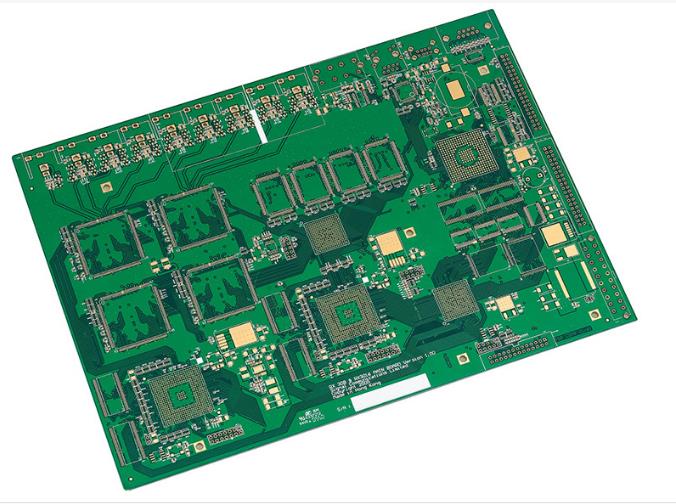
Small batch processing of PCB SMT proofing
SMT proofing small batch processing or PCBA processing process:
1. Single-sided surface assembly process: solder paste printing-patch-reflow soldering.
2. Double-sided appearance assembly process: A side printing solder paste-patch-reflow soldering-flip board-B side printing solder paste-patch-reflow soldering.
3. Single-sided mixed assembly (SMD and THC are on the same side): solder paste printing-patch-reflow soldering-manual plug-in (THC)-wave soldering.
4. Single-sided mixed assembly (SMD and THC are respectively on both sides of the PCB): B-side printing red glue-patch-red glue curing-flap-A side plug-in-B side wave soldering.
5. Double-sided mixed installation (THC has SMD on side A and both sides A and B): Printed solder paste on side A-patch-reflow soldering-flipping board-printed red glue on side B-patch-red glue curing-flipping Board-A side plug-in-B side wave soldering.
6. Double-sided mixed assembly (SMD and THC on both sides of A and B): Printed solder paste on side A-patch-reflow soldering-flip board-printed red glue on side B-patch-red glue curing-flip board-A Surface plug-in-B-side wave soldering-B-side plug-in is attached with computers and related products, communication products and consumer electronics.
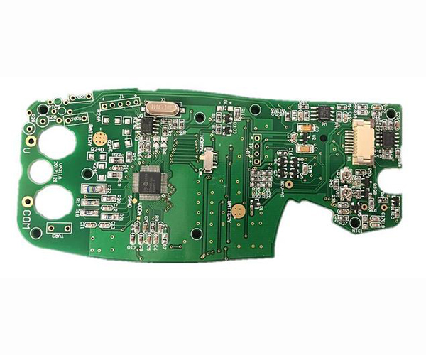
SMT proofing small batch processing
This is the busy process in the usual SMT workshop. Every product must go through strict inspections to ensure that there are no problems with the products in the hands of every customer. It is also a requirement for an excellent PCB manufacturer.