With the rapid development of the semiconductor industry, more and more high-speed, high-function, high-precision packaged devices are applied to the system design of modern car audio, especially the use of high-speed DDR with frequencies above 200MHz in electronic navigation systems, PCB designers are required to achieve strict timing matching in order to achieve the design goals, SI and electromagnetic interference (EMI) design rules to meet the signal integrity of the waveform.
According to the strictness of the design requirements, start with the most important signal lines, in order:
CLK-Data-Address/Command
3.5 Wiring method of CLK differential signal

For the CLK differential signal used in DDR200, the wiring attention points are as follows:
1. The differential impedance should be 100Ω.
2. Differential pair CLK and CLK# should be wired with equal length, but the total length should not be too long.
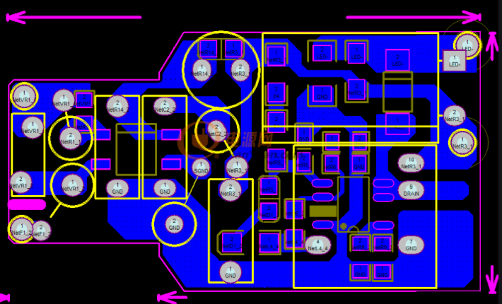
That is, CLK( A-B-C 1-D 1) = CLK( A-B-C1-D2) = CLK( A-B-C 2-D 3) = CLK( A-B-C2-D4) 3.6 DATA The wiring method of the group.
The points to note for PCB wiring are as follows:
1. The length of all D A T A signals starting from N A V I-C P U to each D R A M must be the same (ie A-B-C section).
2. The error of equal-length wiring can be controlled according to the error between the same Bit column and each group of Bits.
3.7 Wiring method of Address/Command
The wiring topology selected by the Address/Command group is marked. The wiring attention points are as follows:
1. The total wiring length (A-B-C-D) is equal in length, and the length error with CLK is controlled within a certain range.
2. The wiring of section D (D1, D2, D3, D4) should be of equal length.
3.8 Design method of equal length wiring
In order to achieve equal length control of network cables such as DATA group, Address/Command group, etc., a curve (or rectangular line) wiring method can be used. However, if the length of the curve is too long or the width DM between the curves is too short, the transmission delay of the signal will be shorter than the expected time due to the coupling between the electromagnetic fields, and the signal will be transmitted to the receiving end prematurely, causing the phenomenon of unequal signal transmission.
3.9 Wiring method of power supply and ground
The power supply used by DDR200 is 2.5V, 3.3V, Vref, Vtt, etc. The wiring attention points are as follows:
1. Vref is used as the reference voltage for the input buffer, and noise from other signals should be avoided. Pay attention to the coupling between the signals of the same layer and the coupling between adjacent upper and lower layers at the same time when wiring. Also avoid mutual interference with Vtt (terminal voltage). Especially in the laminated structure of this example, attention should be paid to the effect of interlayer coupling with the third layer CLK line.
2. In order to reduce the wiring impedance of Vtt and increase the wiring width as much as possible, it is recommended to lay the power surface.
4 Conclusion
This text introduces the PCB design method to realize the high performance of the equipment based on the working principle of DDR200. Nowadays, higher-speed DDR2 and DDR3 have appeared in digital circuits. I hope that the design ideas and high-speed signal wiring methods in this article can be helpful to your design.