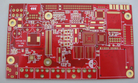
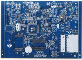
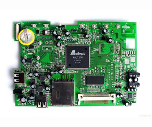
1. Points to note during PCBA processing
PCBA means that the empty PCB board goes through SMT loading, and then goes through the entire process of DIP plug-in, referred to as PCBA. Today we will discuss what needs to be paid attention to during PCBA processing.
1. Transportation: In order to prevent PCBA damage, the following packaging should be used during transportation:
1. Container: anti-static turnover box.
2. Isolation material: anti-static pearl cotton.
3. Placement spacing: there is a distance greater than 10mm between the PCB board and the board, and between the PCB board and the box.
4. Placement height: There is a space greater than 50mm from the top surface of the turnover box to ensure that the turnover box is not pressed against the power supply, especially the power supply of the wire.
2. PCBA processing and washing requirements: the surface of the board should be clean, free of tin beads, component pins, and stains. Especially at the solder joints on the plug-in surface, there should not be any dirt left by soldering.

The following devices should be protected when washing the board: wires, connecting terminals, relays, switches, polyester capacitors and other easily corrosive devices, and the relays are strictly prohibited to be cleaned by ultrasonic.
Need to pay attention to during PCBA processing
3. All components are not allowed to go beyond the edge of the PCB board after installation.
4. When PCBA is processed through the furnace, because the pins of the plug-in components are washed by the tin flow, some plug-in components will be tilted after the furnace is soldered, causing the body of the component to exceed the silk screen frame, so the repair welding personnel after the tin furnace are required to do it Correct appropriately.
1. The horizontal floating high-power resistor can be righted once, and the righting angle is not limited.
2. Horizontal floating diodes (such as DO-201AD packaged diodes) or other components with a component pin diameter greater than 1.2mm can be centered once, and the centering angle is less than 45°.
3. Vertical resistors, vertical diodes, ceramic capacitors, vertical fuses, varistors, thermistors, semiconductors (TO-220, TO-92, TO-247 packages), the bottom of the component body floating height is greater than 1mm It can be centered once, and the centering angle is less than 45°; if the bottom of the component body is less than 1mm, the solder joints must be melted with a soldering iron for centering, or replaced with a new device.
4. In PCBA processing, electrolytic capacitors, manganese copper wires, inductors with skeletons or epoxy board bases, and transformers are not allowed to be righted in principle. Soldering is required once. If there is an inclination, it is required to use a soldering iron to melt the solder joints and then carry out the righting., Or replace with a new device.
2. Process requirements for SMT patch processing
The process requirements for smt patch processing and placement of components. Mounted components should be accurately placed one by one on the printed circuit board in accordance with the requirements of the assembly drawing and schedule of the assembly board.
1. SMT processing and placement process requirements. The type, model, nominal value, polarity and other characteristic marks of each assembly number component on the circuit board must meet the requirements of the product assembly drawing and schedule.
The mounted components must be intact.
The solder ends or pins of smt chip mount components are not less than 1/2 thickness immersed in solder paste. For general components, the amount of solder paste extrusion should be less than 0.2mm during placement, and for fine-pitch components, the amount of solder paste extrusion should be less than 0.1mm during placement.
The solder ends or pins of the components should be aligned and centered with the land pattern. Due to the self-alignment effect of reflow soldering, a certain deviation is allowed during component mounting. For the specific deviation range of various components, please refer to the relevant IPC standards.
2. Three elements to ensure the quality of PCB circuit board mounting.
1. The components are correct. It is required that the type, model, nominal value and polarity of each assembly tag component must meet the requirements of the product assembly drawing and schedule, and cannot be pasted in the wrong position.
2. The location is accurate. The solder ends or pins of the components are aligned and centered with the land pattern as much as possible, and the solder ends of the components must be in contact with the solder paste pattern.
3. The pressure is right. The placement pressure is equivalent to the Z-axis height of the nozzle, the high Z-axis height is equivalent to the small placement pressure, and the low Z-axis height is equivalent to the high placement pressure. If the height of the second axis is too high, the solder end or pin of the component does not press the solder paste, and floats on the surface of the solder paste, the solder paste cannot stick to the component, and it is prone to position shift during transmission and reflow soldering.
In addition, the height of the Z axis is too high, which makes the components fall freely from a high place during placement, which will cause the placement of the placement to shift. On the contrary, if the height of the second axis is too low and the amount of solder paste squeezed out is too much, it is easy to cause solder paste adhesion, and bridging is prone to occur during reflow soldering. At the same time, the slip of the alloy particles in the solder paste will cause the patch position to shift. It will also damage components. Therefore, the Z-axis height of the suction nozzle is required to be appropriate and appropriate during placement.