CPU chip packaging technology and packaging method:
CPU packaging technology is divided into dip packaging, QFP packaging, PFP packaging, PGA packaging, BGA packaging, etc.
CPU package forms: OPGA package, MPGA package, CPGA package, FC-PGA package, fc-pga2 package, Ooi package, PPGA package, s.e.c.c. package, s.e.c.2 package, s.e.p. package, PLGA package, cupga package, etc.
1, First, explain the CPU packaging technology
DIP pcckage(DualIn-linePackage):
Also known as dual in-line packaging technology, it refers to integrated circuit chips packaged in dual in-line form. Most small and medium-sized integrated circuits adopt this packaging form, and the number of pins generally does not exceed 100. The CPU chip in dip package has two rows of pins, which need to be inserted into the chip socket with dip structure. Of course, it can also be directly inserted into the circuit board with the same number of welding holes and geometric arrangement for welding. When the chip of dip package is plugged from the chip socket, special care shall be taken to avoid damaging the pin. Dip packaging structure forms include: multi-layer ceramic dual in-line dip, single-layer ceramic dual in-line dip, lead frame dip (including glass ceramic sealing, plastic packaging structure, ceramic low melting glass packaging), etc.
Dip package features:
1. It is suitable for perforation welding on PCB (printed circuit board) and easy to operate.
2. The ratio between chip area and package area is large, so the volume is also large.
The early 4004, 8008, 8086, 8088 and other CPUs adopt dip package, which can be inserted into the slot on the motherboard or welded on the motherboard through two rows of pins.
QFP package:
The Chinese meaning of this technology is called square flat packaging technology. The distance between CPU chip pins realized by this technology is very small and the pins are very thin. This packaging form is generally adopted for large-scale or very large-scale integrated circuits, and the number of pins is generally more than 100.
QFP package features:
This technology is easy to operate and reliable when packaging CPU; Moreover, the package size is small and the parasitic parameters are reduced, which is suitable for high-frequency applications; This technology is mainly suitable for mounting and wiring on PCB with SMT surface mounting technology.
PFP package:
The full English name of this technology is plastic flatpackage, and the Chinese meaning is plastic flat component package. The chip packaged with this technology must also be welded with the motherboard by SMD technology. The chip installed with SMD does not have to punch on the main board. Generally, there are designed pads of corresponding pins on the surface of the main board. Align each pin of the chip with the corresponding pad to realize the welding with the motherboard. The chip welded in this way is difficult to disassemble without special tools. This technology is basically similar to the above QFP technology, but the package shape is different.
PGA package:
This technology is also called the ceramic pin grid array package technology. There are multiple square array pins inside and outside the chip encapsulated by this technology. Each square array pin is arranged at a certain distance around the chip, and can be surrounded by 2 ~ 5 circles according to the number of pins. When installing, insert the chip into a special PGA socket. In order to make the installation and disassembly of the CPU more convenient, a zifcpu socket has emerged from the 486 chip, which is specially used to meet the installation and disassembly requirements of the CPU packaged by PGA. This technology is generally used in situations where plugging operations are frequent.
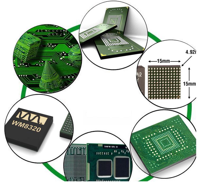
BGA package:
BGA Technology (ball grid array package) is ball grid array packaging technology. The emergence of this technology has become a good choice for high-density, high-performance and multi pin packaging such as CPU, motherboard South and North Bridge chips. However, BGA packaging occupies a large area of the substrate. Although the number of I / O pins of this technology increases, the distance between pins is much greater than QFP, which improves the assembly yield. Moreover, the technology adopts controllable collapse chip welding, which can improve its electrothermal performance. In addition, the technology can be assembled by coplanar welding, which can greatly improve the reliability of packaging; The encapsulated CPU realized by this technology has small signal transmission delay and can greatly improve the adaptive frequency.
BGA package features:
1. Although the number of I / O pins increases, the distance between pins is much greater than that of QFP packaging, which improves the yield
2. Although the power consumption of BGA increases, the electrothermal performance can be improved due to the controllable collapse chip welding method
3. The signal transmission delay is small and the adaptive frequency is greatly improved
4. Coplanar welding can be used for assembly, and the reliability is greatly improved

CPU packaging technology is divided into dip packaging, QFP packaging, PFP packaging, PGA packaging, BGA packaging
2, Next, let's talk about the packaging forms, which are common at present
OPGA package(OrganicpingridArray)
The substrate of this package is glass fiber, similar to the material on printed circuit boards. This kind of packaging method can reduce the impedance and packaging cost. OPGA package can improve the power supply and filter current clutter of the core by closing the distance between the external capacitance and the processor core. AMD's athlonxp series CPUs mostly use such encapsulation.
MPGA package
MPGA, micro PGA package, is only adopted by a few products such as Athlon64 of AMD company and Xeon (Xeon) Series CPU of Intel company, and most of them are excellent products, which is an advanced packaging form.
CPGA package
CPGA, also known as ceramic packaging, is fully known as ceramicpga. It is mainly used on the Athlon processor of Thunderbird core and "Palomino" core.
FC-PGA package
FC-PGA package is the abbreviation of reverse chip pin grid array. This package has pins inserted into the socket. These chips are reversed so that the chip die or the processor part constituting the computer chip is exposed on the upper part of the processor. By exposing the die, the thermal solution can be directly applied to the die, which can achieve more effective chip cooling. In order to improve the performance of the package by isolating the power signal and grounding signal, the FC-PGA processor has discrete capacitors and resistors installed in the capacitor placement area (processor Center) at the bottom of the processor. The pins at the bottom of the chip are zigzag. In addition, the pins are arranged so that the processor can only be inserted into the socket in one way. The FC-PGA package is used for Pentium III and Intel Celeron processors, both of which use 370 pins.
Fc-pga2 package
The fc-pga2 package is similar to the FC-PGA package type, except that these processors also have an integrated heat sink (IHS). The integrated heat sink is directly installed on the processor chip during production. Because IHS has good thermal contact with the die and provides a larger surface area to better dissipate heat, it significantly increases heat conduction. The fc-pga2 package is used for Pentium III and Intel Celeron processors (370 pins) and Pentium 4 processors (478 pins).
OOI package
Ooi is short for Olga. Olga represents the substrate grid array. Olga chip also uses reverse chip design, in which the processor is attached to the substrate downward to achieve better signal integrity, more effective heat dissipation and lower self induction. An integrated heat sink (IHS) is installed to help transfer heat to the correct heat sink. Ooi is used for Pentium 4 processors, which have 423 pins.
PPGA package
The full English name of "PPGA" is "plastic pingridarray", which is the abbreviation of plastic pin grid array. These processors have pins inserted into sockets. In order to improve the thermal conductivity, PPGA uses a nickel plated copper radiator on the top of the processor. The pins at the bottom of the chip are zigzag. In addition, the pins are arranged so that the processor can only be inserted into the socket in one way.
S.E.C.C. package
"S.E.C.C." is the abbreviation of "single edge contact cartridge", which is the abbreviation of single side contact cartridge. To connect to the motherboard, the processor * * is inserted into a slot. Instead of using pins, it uses "golden finger" contacts that the processor uses to transmit signals. S. The top of the E.C. box is covered with a metal shell.
The back of the card box is a hot material coating, which acts as a radiator. S. Inside e.c.c., most processors have a printed circuit board called the matrix, which connects the processor, L2 cache and bus termination circuit. S. The e.c.c. package is used for Intel Pentium II processors with 242 contacts and Pentium II Xeon and Pentium III Xeon processors with 330 contacts.
S.E.C.C.2 package
The S.E.C.C.2 package is similar to the s.e.c.c. package, except that s.e.c.c.2 uses less protective packaging and does not contain thermal conductive coatings. S. The S.E.C.C.2 package is used for some later versions of Pentium II processors and Pentium III processors (242 contacts).
S.E.P. package
"S.E.P." is the abbreviation of "single edge processor", which is the abbreviation of single-sided processor“ S. The "E.P." package is similar to the "s.e.c.c." or "s.e.c.2" package. It is also inserted into the slot on one side and contacts the slot with a gold finger. However, it does not have a fully packaged shell, and the backplane circuit is visible from the bottom of the processor“ S.E.P. "package was applied to the early 242 golden finger Intel Celeron processors.
PLGA package
PLGA is the abbreviation of plastic landgridarray, that is, plastic pad grid array packaging. Because pins are not used, but small dot interfaces are used, PLGA package obviously has smaller volume, less signal transmission loss and lower production cost than previous fc-pga2 packages, which can effectively improve the signal strength and frequency of the processor, improve the yield of processor production and reduce the production cost. At present, the CPU of Socket 775 interface of Intel company adopts this package.
CuPGAa package
CuPGA is the abbreviation of lidded ceramic packaging grid array, that is, covered ceramic grid array packaging. The big difference between it and ordinary ceramic package is the addition of a top cover, which can provide better heat dissipation performance and protect the CPU core from damage. At present, AMD64 Series CPU adopts this package.

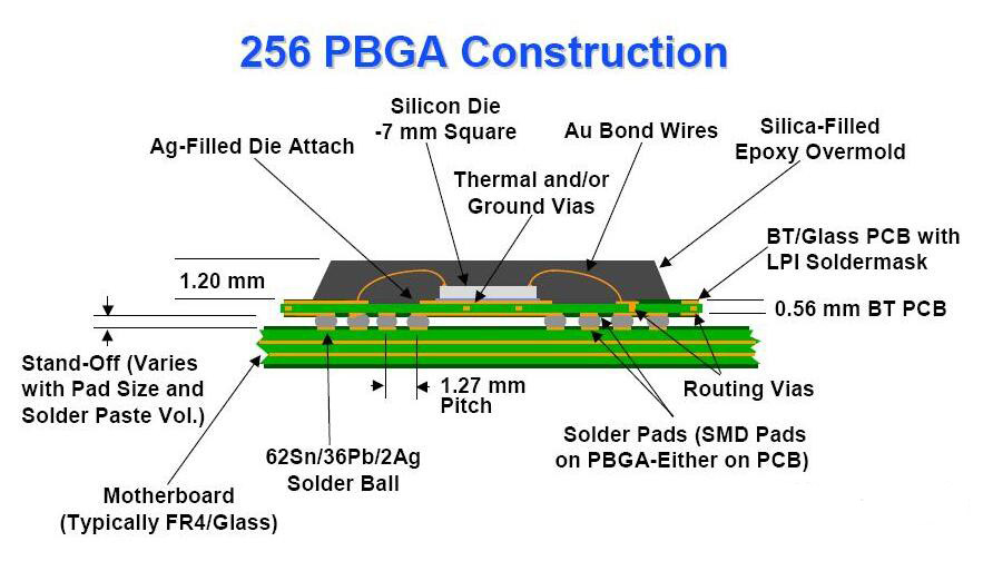
256 PBGA Construction
The article comes from (www.ipcb.com) IPCB is a professional R&D and manufacturer of high-precision PCB circuit boards. It can mass produce 4-46 layers of PCB boards, circuit boards, CPU circuit boards, high-frequency boards, high-speed boards, HDI boards, PCB circuit boards, high-frequency high-speed boards, IC packaging carrier boards, semiconductor test boards, multi-layer circuit boards, HDI circuit boards, mixed voltage circuit boards, high-frequency circuit boards, soft and hard combination boards, etc.