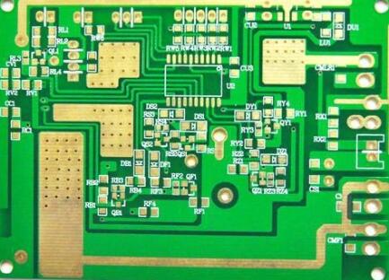
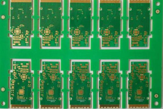
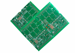
The following is an introduction to the rapid placement of advanced packaging devices on PCB circuit boards
As surface array packaging is becoming more and more important, especially in the fields of automotive, telecommunications and computer applications, productivity has become the focus of discussion. The pin pitch is less than 0.4mm, which is 0.5mm. The main problem of fine pitch QFP and TSOP packages is low productivity. However, since the pitch of the area array package is not very small (for example, the flip chip is less than 200 μm), after reflow soldering, the dmp rate is at least 10 times better than the traditional fine-pitch technology. Furthermore, compared with the QFP and TSOP packages of the same pitch, considering the automatic alignment during reflow soldering, the mounting accuracy requirements are much lower.
Another advantage, especially the flip chip, the footprint of the PCB printed circuit board is greatly reduced. The surface array package can also provide better circuit performance.
Therefore, the industry is also developing in the direction of surface array packaging. μBGA with a minimum pitch of 0.5mm and chip-scale package (CSP) are constantly attracting people’s attention. At least 20 multinational companies are working on this. Research on a series of packaging structures. In the next few years, it is expected that the consumption of bare chips will increase by 20% every year. The fastest growing rate will be flip-chip chips, followed by bare chips used in COB (Direct Mounting on Board).

It is estimated that the consumption of flip-chip chips will increase from 500 million in 1996 to 2.5 billion at the end of this century, while the consumption of TAB/TCP stagnated or even showed negative growth. As expected, it was only about 700 million in 1995.
PCB mounting method
The mounting requirements are different, and the mounting method (principle) is also different. These requirements include component pick-and-place capability, placement strength, placement accuracy, placement speed, and flux fluidity. When considering placement speed, one of the main characteristics to consider is placement accuracy.
Pick and place
The fewer the placement heads of the placement equipment, the higher the placement accuracy. The accuracy of the positioning axes x, y and θ affects the overall placement accuracy. The placement head is mounted on the support frame of the placement machine's xy plane. The most important part of the placement head is the rotation axis, but do not ignore the movement accuracy of the z axis. . In the high-performance placement system, the movement of the z-axis is controlled by a microprocessor, and the vertical movement distance and placement force are controlled by sensors.
One of the main advantages of placement is that the precision placement head can move freely in the x and y planes, including taking materials from the waffle disk, and performing multiple measurements on the device on a fixed upward-looking camera.
The most advanced placement system can achieve 4 sigma and 20μm accuracy on the x and y axes. The main disadvantage is that the placement speed is low, usually less than 2000 cph, which does not include other auxiliary actions, such as flip chip coating flux. Wait.
The simple placement system with only one placement head will soon be eliminated and replaced by a flexible system. In such a system, the support frame is equipped with a high-precision placement head and a revolver head, which can mount large-size BGA and QFP packages. The rotating (or shooter) head can handle irregularly shaped devices, fine-pitch flip-chip chips, and μBGA/CSP chips with pin pitches as small as 0.5mm. This placement method is called "collect, pick and place".
High-performance SMD placement equipment equipped with flip chip spin heads has appeared on the market. It can mount flip-chips and μBGA and CSP chips with a ball grid diameter of 125μm and a pin pitch of about 200μm at high speed. The placement speed of equipment with collecting, picking and placement functions is about 5000cph.
Traditional wafer sniffer
Such a system has a rotating head that rotates horizontally while picking up components from a moving feeder and attaching them to the moving PCB circuit board. Theoretically, the placement speed of the system can reach 40,000cph, but it has the following limitations:
Wafer picking cannot exceed the grid plate where the device is placed;
The spring-driven vacuum nozzle does not allow work-hour optimization during the movement of the z-axis, or cannot reliably pick up the die from the conveyor belt;
For most surface array packages, the placement accuracy cannot meet the requirements, and the typical value is higher than 10μm at 4sigma;
Can not realize the application of soldering flux for micro flip chip.
Collection and placement
In the "collect and place" sniffer system, both rotating heads are mounted on the x-y support frame. Then, the rotating head is equipped with 6 or 12 suction nozzles, which can touch any position on the grid plate. For standard SMD chips, this system can achieve a placement accuracy of 80μm and a placement speed of 20,000pch at 4sigma (including theta deviation). By changing the positioning dynamic characteristics of the system and the search algorithm of the ball grid, for the surface array package, the system can achieve a placement accuracy of 60μm to 80μm and a placement speed higher than 10,000pch under 4sigma.
Placement accuracy
In order to have an overall understanding of different placement equipment, you need to know the main factors that affect the placement accuracy of the area array package. Ball grid placement accuracy P\/\/ACC\/\/ depends on the type of ball grid alloy, the number of ball grids and the weight of the package.
These three factors are interrelated. Compared with ICs in QFP and SOP packages with the same pitch, most surface array packages have lower mounting accuracy requirements. Note: Insert equation
For round pads without solder mask, the maximum allowable mounting deviation is equal to the radius of the PCB pad. When the mounting error exceeds the radius of the PCB pad, there will still be mechanical contact between the ball grid and the PCB pad. Assuming that the diameter of the usual PCB pad is roughly equal to the diameter of the ball grid, the placement accuracy of the μBGA and CSP packages with a ball grid diameter of 0.3mm and a pitch of 0.5mm is required to be 0.15mm; if the ball grid diameter is 100μm and the pitch is 175μm, The accuracy requirement is 50μm.
In the case of tape ball grid array packages (TBGA) and heavy ceramic ball grid array packages (CBGA), self-alignment is limited if it occurs. Therefore, the precision requirements for placement are high.
Application of flux
The furnace used for standard large-scale reflow soldering of flip chip ball grids requires flux. Nowadays, the more powerful general-purpose SMD placement equipment has built-in flux application devices, and the two commonly used built-in supply methods are coating and dip soldering.
The coating unit is installed near the placement head. Before flip chip placement, apply flux to the placement position. The dose applied in the center of the mounting position depends on the size of the flip chip and the wetting characteristics of the solder on the specific material. It should be ensured that the flux coating area is large enough to avoid missing pads due to errors.
In order to perform effective filling in a non-cleaning process, the flux must be a non-cleaning (no residue) material. Liquid flux always contains very little solid matter, and it is most suitable for non-cleaning processes.
However, due to the fluidity of the liquid flux, after flip chip placement, the movement of the placement system conveyor belt will cause the inertial displacement of the chip. There are two ways to solve this problem:
Before the PCB board is transferred, set a waiting time of several seconds. During this time, the flux around the flip chip evaporates quickly to improve the adhesion, but this will reduce the yield.
You can adjust the acceleration and deceleration of the conveyor belt to match the adhesion of the flux. The smooth movement of the conveyor belt will not cause wafer displacement.
The main disadvantage of the flux coating method is that its cycle is relatively long. For each device to be coated, the mounting time increases by about 1.5s.
PCB dip soldering method
In this case, the flux carrier is a rotating bucket, and a blade is used to scrape it into a flux film (about 50μm). This method is suitable for high-viscosity flux. By only dipping the solder on the bottom of the ball grid, the consumption of solder can be reduced during the manufacturing process.