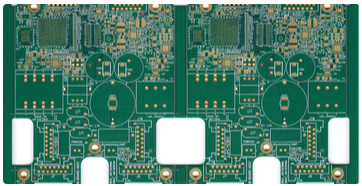
High frequency circuit board wiring
1. The shorter the lead between the pins of the high-frequency circuit board device, the better
The radiation intensity of the signal is proportional to the trace length of the signal line. The longer the high-frequency signal lead, the easier it is to couple to the components close to it. Therefore, for signals such as clock, crystal oscillator, DDR data, LVDS lines, USB lines, HDMI lines and other high-frequency signal lines are required to be as short as possible.
2. The less the lead layer alternate between the pins of the high-frequency circuit device, the better
The so-called "the less the inter-layer alternation of the leads, the better" means that the fewer vias (Via) used in the component connection process, the better. According to the side, one via can bring about 0.5pF distributed capacitance, and reducing the number of vias can significantly increase the speed and reduce the possibility of data errors.
3. Pay attention to the "crosstalk" introduced by the signal lines in parallel with close distances
High-frequency circuit wiring should pay attention to the "crosstalk" introduced by the close parallel routing of signal lines. Crosstalk refers to the coupling phenomenon between signal lines that are not directly connected. Since high-frequency signals are transmitted in the form of electromagnetic waves along the transmission line, the signal line will act as an antenna, and the energy of the electromagnetic field will be emitted around the transmission line. Undesirable noise signals are generated due to the mutual coupling of electromagnetic fields between the signals. Called crosstalk (Crosstalk). The parameters of the PCB layer, the spacing of the signal lines, the electrical characteristics of the driving end and the receiving end, and the signal line termination method all have a certain impact on the crosstalk. Therefore, in order to reduce the crosstalk of high-frequency signals, it is required to do the following as much as possible when wiring:
If the wiring space permits, inserting a ground wire or ground plane between the two wires with more serious crosstalk can play a role in isolation and reduce crosstalk.
When there is a time-varying electromagnetic field in the space surrounding the signal line, if parallel distribution cannot be avoided, a large area of "ground" can be arranged on the opposite side of the parallel signal line to greatly reduce interference.
On the premise that the wiring space permits, increase the spacing between adjacent signal lines, reduce the parallel length of the signal lines, and try to make the clock line perpendicular to the key signal line instead of parallel.
If parallel wiring in the same layer is almost unavoidable, in two adjacent layers, the directions of the wiring must be perpendicular to each other.
In digital circuits, the usual clock signals are signals with fast edge changes, which have high external crosstalk. Therefore, in the design, the clock line should be surrounded by a ground line and punched more ground line holes to reduce distributed capacitance, thereby reducing crosstalk.
For high-frequency signal clocks, try to use low-voltage differential clock signals and wrap the ground mode, and pay attention to the integrity of the package ground punching.
The unused input terminal should not be suspended, but grounded or connected to the power supply (the power supply is also grounded in the high-frequency signal loop), because the suspended line may be equivalent to the transmitting antenna, and the grounding can inhibit the emission. Practice has proved that using this method to eliminate crosstalk can sometimes yield immediate results.

4. Add high-frequency decoupling capacitor to the power supply pin of the integrated circuit block
A high-frequency decoupling capacitor is added to the power supply pin of each integrated circuit block nearby. Increasing the high-frequency decoupling capacitor of the power supply pin can effectively suppress the interference of high-frequency harmonics on the power supply pin.
PCB design and manufacturing package
1. Speed up and improve PCB wiring
Traditional PCB wiring is limited by fixed wire coordinates and lack of wires at any angle. Removing these restrictions can significantly improve the quality of the wiring. This article will introduce the advantages of arbitrary-angle wiring, the advantages of flexible wiring, and a new algorithm for constructing Steiner trees through practical examples.
2. What issues should be paid attention to when drawing PCB diagrams from the perspective of welding?
Although there are more sophisticated placement machines that can replace manual welding, there are too many factors that affect the quality of welding. This article introduces several points that need to be paid attention to when designing PCB from the perspective of patch soldering. According to experience, if these requirements are not followed, it is likely to cause poor soldering quality, false soldering, and even damage to the soldering during PCB repair. Disk or circuit board.
3. Wiring skills and essentials when drawing PCB
Wiring is the finest and most restrictive technique in the PCB design process. Here are some good wiring techniques and essentials.
PCB simulation and design of DDR3 memory
The main factors affecting signal integrity are analyzed for DDR3 timing, and the analysis results are used to improve and optimize the design.