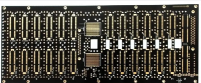
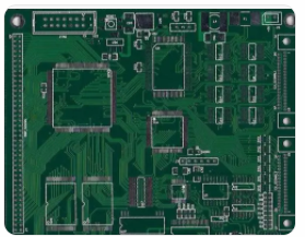
The current electronic design of PCB proofing is mostly integrated system-level design, and the whole project includes both hardware design and software development. This technical feature poses new challenges to PCB engineers.

First of all, how to divide the system's software and hardware functions reasonably in the early design stage to form an effective functional structure framework to avoid redundant cyclic processes;
Secondly, how to design a high-performance and high-reliability PCB board in a short time. Because the development of software relies heavily on the realization of hardware, only by ensuring that the whole machine design is passed once can the design cycle be shortened more effectively. This article discusses the new features and new strategies of system board-level design under the new technical background.
As we all know, the development of electronic technology is changing with each passing day, and the root cause of this change is the progress of chip technology. The semiconductor process is becoming increasingly physical, and has now reached the deep sub-micron level, and ultra-large-scale circuits have become the mainstream of chip development. And this change in process and scale has brought many new electronic design bottlenecks throughout the entire electronics industry. The board-level design has also been greatly impacted. The most obvious change is the huge variety of chip packaging, such as the emergence of BGA, TQFP, PLCC and other packaging types; secondly, high-density pin packaging and miniaturized packaging have become one. This kind of fashion, in order to realize the miniaturization of the whole product, such as: the wide application of MCM technology. In addition, the increase in the operating frequency of the chip makes it possible to increase the operating frequency of the system. These changes will inevitably bring many problems and challenges to board-level design. First, due to the increasing physical limits of high-density pins and pin sizes, resulting in low deployment rates; secondly, the timing and signal integrity problems caused by the increase in system clock frequency; thirdly, engineers hope to be able to use the PC platform Use better tools to complete complex and high-performance designs. Therefore, it is not difficult for us to see that PCB board design has the following three trends:
The PCB design of high-speed digital circuits (that is, high clock frequency and fast edges) has become the mainstream.
Product miniaturization and high performance must face the problem of distribution effects caused by mixed-signal design technology (ie, digital, analog, and RF mixed design) on the same board.
The increase in design difficulty has caused the traditional design process and design methods, and the CAD tools on the PC to be difficult to meet the current technical challenges. Therefore, the transfer of the EDA software tool platform from the UNIX to the NT platform has become a recognized trend in the industry.
PCB board solution for high-speed digital system of PCB proofing
In general, when the signal interconnection delay is greater than 20% of the edge signal flipping threshold time, the signal wire on the board will show the transmission line effect, that is, the connection is no longer a simple wire showing lumped parameters Performance, but showing the effect of distributed parameters, this design is a high-speed design. In the design of high-speed digital systems, designers must solve the problem of false flipping and signal distortion caused by parasitic parameters-that is, timing and signal integrity issues. At present, this is also a bottleneck problem that high-speed circuit designers must solve.
PCB proofing is driven by traditional physical rules
We can find that in traditional high-speed PCB circuit design, electrical rule setting and physical rule setting are separate. This brings the following shortcomings:
In the early days of PCB design, engineers had to spend a lot of energy on detailed front-end and back-end (that is, logic establishment-physical realization) analysis to plan a physical wiring strategy that meets electrical requirements.
The high-speed effect is a complicated subject, and the expected effect cannot be achieved simply by controlling the wiring length and parallel lines.
The designer will inevitably face such a dilemma. The physical rules with false components are not applicable in actual wiring. He has to modify the rules repeatedly to make them have practical value.
When the wiring is completed, the post-verification tool can be used for analysis. But if a problem is found, the engineer must return to the design and adjust the structure or rules. This is a cyclic redundant process. It will inevitably affect the time to market.
When there are only a few or dozens of critical wire nets in the design, the physical rule drive can complete the design task well; but when there are hundreds or even thousands of wire nets in the design, the physical rule-driven method is fundamental Inability to perform design tasks. The development of electronic technology calls for the emergence of new methods and tools to solve the bottleneck problems faced by the design. In order to solve the shortcomings of physical rule-driven high-speed design, people of insight in the industry engaged in the development of high-speed digital circuit design EDA tools proposed the concept of real-time electrical rule-driven physical layout three years ago, and designed high-speed digital PCB design ideas. The process was reformed.