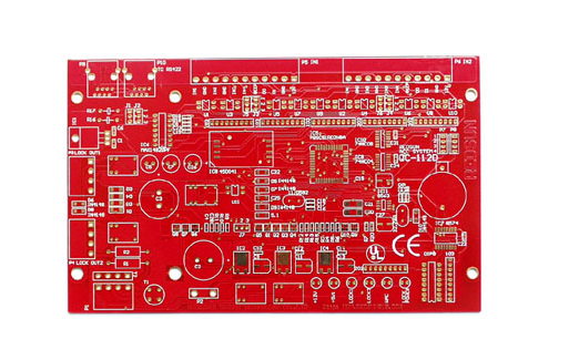
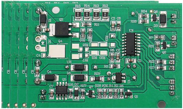
We will design a fully user-friendly wifi antenna PCB with ESP8266 wifi module. Now we will discuss the circuit diagram. Now, as we said before, before designing any circuit, you should read the hardware design guide. You can download it from Google.
First, we must design the circuit diagram of the ESP8266 development board with all possible connections and components.
Components required for the circuit diagram:
ESP8266 WiFi module (ESP-01)
Female head (some strips)
Button
1KΩ (1/4 Watt) resistance
2KΩ resistance (1/4 watt)
100 nF capacitor
Two-way slide switch
When using the ESP8266 wifi module, we must understand the pin configuration of the ESP8266 ESP-01 variant. It has 8 pins, such as VCC, GND, TX, RX, GPIO0, GPIO2, RST (reset) and CH_PD.

The VCC and CH_PD pins are connected to the VCC of the power header connector, and the GND pin is connected to the GND terminal.
The RST pin is connected to the button and GND.
GPIO2 is connected to the female GPIO header connector. On the other hand, GPIO0 is connected to the center terminal of the two-way slide switch.
The TX pin is directly connected to the TX pin of the communication socket. The RX pin is connected to a level shifter composed of 1kohm and 2.2kohm resistors.
We will design the scheme according to the circuit diagram.
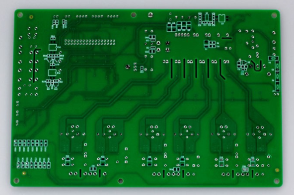
The schematic is complete and you can see that it is a very simple design. Therefore, let us design a single-layer printed circuit board.
Now, we have to send this design to the PCB manufacturer to make the PCB into our design, and then we will assemble all the components and then it is ready to use.
To use it, just connect the 3.3v power supply to the VCC and GND pins. Now, if you want to program it with firmware, just switch to the programming mode position and press the RST button.
What is the Bluetooth antenna PCB?
The steps required to construct the Bluetooth antenna PCB.
design concept:
Before designing the Bluetooth antenna PCB, please read the Internet guide carefully and create a concept about it, so that you can visualize everything. The Bluetooth circuit is the core part of Bluetooth, including ICs, capacitors, power points and other components. The working frequency of Bluetooth connection is 2.4 GHz. As we all know, in Bluetooth operation, there is at least one master device and one or more slave devices.
Bluetooth circuit board:
The Bluetooth circuit board must contain at least one antenna that helps to send and receive information. In order to improve the performance of the Bluetooth circuit board, we must use at least two inductors that can adjust the antenna impedance.
We said before that the Bluetooth PCB works in the 2.4 GHz range, which is also the radio frequency range that we also use in Wi-Fi technology. We know that Bluetooth communication has a master device and one or more slave devices, but we must remember that the number of slave devices we can use is 7. The master device and the slave device can work within a distance of up to 10 meters. Bluetooth devices always work by exchanging some unique codes, so to use Bluetooth, we need to get approval from the master and the slave. The PCB near the antenna may cause a lower resonance frequency, so it is always recommended to keep the thickness of the PCB for Bluetooth at 1.6mm.
Bluetooth transmitter circuit: The Bluetooth transmitter circuit is mainly related to data transmission. It also helps to pair your Bluetooth device with other devices. It contains components that include LED indicators so that you can indicate when the device is connected to other devices. The main battery is protected by a small circuit, so overcurrent will not damage the device. The Bluetooth transmitter circuit also includes a voltage regulator, battery charging unit, USB module and so on.
You can use two types of batteries to power the Bluetooth circuit board. You can use 1A USB power supply or LiPo battery. The dashboard is also composed of led lights and sound installation, so you can indicate the connection status.
Some features of the Bluetooth circuit board include:
It contains a sound device and led lights, which can indicate the connection status at any time.
Allow multiple devices to seamlessly transfer data using wireless connections.
Its design is simple and the programming is so smart that users can use it without knowing it. The user interface of any Bluetooth device is very easy to use.
The Bluetooth antenna PCB is designed in such a way that you can connect to the last paired device or the nearest device in the preferred range.
How to make Bluetooth antenna PCB:
Therefore, first we must design the schematic diagram. PCB design is one of the most challenging parts. If you are good at PCB design, it will be the perfect choice. When designing the Bluetooth antenna PCB, we must keep some things in mind.
1. First, we need a Bluetooth head, amplifier, switch, LED and a box. We must ensure that the cable does not pass through the head, as this will reduce the range of the Bluetooth.
Try to place the system away from the transmitter, because if it is placed close to the transmitter in any way, it may affect the normal transmission process.
You must choose the number of layers based on the number of functions you want to add to the board. It is generally recommended that you choose a multi-layer design for the Bluetooth PCB.
After the design is completed, send it to the PCB manufacturer to manufacture according to your design. Then assemble all the necessary components, and then you can start.