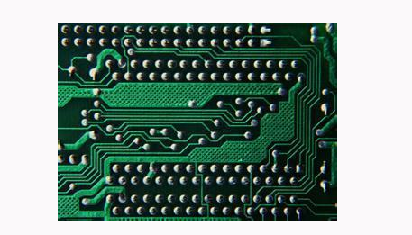
The skin depth in PCB and its interaction with the final surface treatment
Skin depth usually refers to the depth of the conductor in the radio frequency RF circuit board where the current is located. Imagine that by observing the cross-section of a circular wire, you can see where current flows through the cross-section. If the current is provided by the battery of direct current (DC), the current density is uniformly distributed across the cross section of the wire, and the current density is the same everywhere in the wire area.
If you change the current source to sinusoidal alternating current, you will find that the current density at the outer edge of the wire is greater than the current density in the middle of the wire. As the frequency continues to increase, you will notice that at some points in the middle of the cross-sectional area of the wire, no current flows, and most of the current will be concentrated on the outer edge of the conductor (the outer surface of the conductor). This is the basic concept of skin depth.
The following formula will help us understand which factors are related to skin depth. The simple definition of skin depth (ð) is:
ð = (1/(π*f*µ*σ))0.5 (Formula 1)
Among them: π is the circumference ratio, which is a fixed constant, f is the frequency, μ is the magnetic permeability, and σ is the electrical conductivity.
It is estimated that most people will be a little confused when they see this formula for the first time. But in fact this formula is easy to understand. The value of the symbol "μ" in the formula is related to the magnetic properties of the metal, and the relative value of copper is about 1, so the magnetic permeability of copper has no effect on the equation. The value of the symbol "σ" in the formula is related to the conductivity of the metal. Copper is one of the metals with the best conductivity (high conductivity).

From Formula 1, you can easily see the relationship between skin depth and various variables. For example: as the frequency "f" increases (higher frequency), the skin depth "ð" will become smaller. The same is true: if you use a metal with a lower conductivity "σ", the skin depth will become larger, which is what happens when certain types of final surface treatments are applied to the PCB conductor.
Skin depth and its interaction with the final surface treatment
A special surface treatment method commonly used in industry is chemical nickel gold (ENIG). The influence of ENIG is related to the edge effect of the conductor. At the edge of the conductor where the conductor is in contact with the substrate, there will naturally be a higher current density, and the difference in the conductivity of the edge metal will result in a difference in radio frequency performance. Under ENIG's processing technology, it is assumed that at very low frequencies where the skin depth is very thick, the conductivity at the edge of the conductor is a composite conductivity composed of copper-nickel-gold. As the frequency increases, the composite conductivity will be determined by nickel-gold. At very high frequencies, the conductivity will only be related to the gold-plated layer.
In order to let you know the conductivity of different metals, we give the value of several common metals (unit is 107S/m), copper is 5.8, nickel is 1.5, and gold is 4.5. In fact, these values only apply to pure metals. In actual circuits, these metals used for PCB processing are usually alloys, and their conductivity will be slightly different, but these are good reference values. It can be seen that the conductivity of nickel is about 1/4 of that of copper, so this is also a double-edged sword for radio frequency problems. Lower conductivity will result in greater insertion loss, and will also increase the skin depth, which means that the RF current flows through more lossy metal.
ENIG has another problem, which is the potential problem related to "magnetism". The relative permeability (μ) of pure nickel is very high, about 500, but the nickel used in ENIG is an alloy with a lower μ value than pure nickel - but its value is still very large. As μ increases, it can be seen from the skin depth formula that the skin depth will decrease. This is a counteracting factor for the lower conductivity of nickel. There are also metal-related magnetic losses. Nickel does have higher magnetic losses than copper. It is similar to the loss related to the dielectric. The dielectric loss is related to the loss factor (Df), and the magnetic loss is similar to it, related to the magnetic properties of the metal.
The following is an actual engineering case related to ENIG and skin depth. A customer told us that when they tested the performance of multiple circuit boards of the same design, they found that the RF losses of these circuits were significantly different. This is basically a change between different circuits. The results further found that the operating frequency of these circuits is 800MHz (0.8 GHz), which is an interesting frequency because it involves the skin depth associated with ENIG.
At this frequency, the skin depth of copper is approximately 2.3 microns (approximately 92 microinches), while for ENIG, it is slightly thicker. Affected by many factors, ENIG's nickel layer can range from 50-250 microinches. Under normal circumstances, ENIG's circuit-to-circuit changes are not so extreme, but ENIG's normal nickel thickness changes will vary due to many different reasons.
The results show that the thickness change of nickel has a certain effect on the skin depth change within the appropriate thickness range, which is the reason why the composite conductivity of copper, nickel and gold varies with the thickness of nickel. At this frequency of 800MHz, changes in nickel thickness have a significant impact on skin depth and related insertion loss. However, if the application at the frequency of 24 GHz, the skin depth is about 17 micro inches, the composite metal conductor will not affect the performance of the circuit, because the composite metal of ENIG is composed of only about 8 micro inches of gold, and the rest All are nickel. Finally, of course, this is just an example of ENIG at the edge of a conductor affecting insertion loss.