Origin of PCB
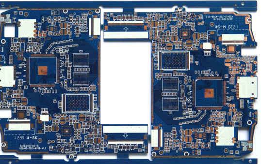
The contemporary magic pen Ma Liang mentioned today is Paul Eisler, the father of PCB. He is an Austrian, PCB-Printed Circuit Board. Printed circuit boards, also known as printed circuit boards, are important electronic components and supports for electronic components, as well as a carrier for electrical connections of electronic components. Because it is made by electronic printing, it is called a "printed" circuit board. He used a printed circuit board in a radio in 1936.
Modern electronic equipment cannot do without printed circuit boards, so what are the benefits of it? The main advantages of using printed boards are:
1. Due to the repeatability (reproducibility) and consistency of the graphics, the errors in wiring and assembly are reduced, and the maintenance, debugging and inspection time of the equipment is saved;
2. The design can be standardized to facilitate interchange;
3. The wiring density is high, the volume is small, and the weight is light, which is conducive to the miniaturization of electronic equipment;
4. Facilitate mechanization and automated production, improve labor productivity and reduce the cost of electronic equipment.
What is the circuit board made of?
The current circuit board mainly consists of the following:
Circuit and pattern (Pattern): The circuit is used as a tool for conduction between the originals. In the design, a large copper surface will be additionally designed as a grounding and power layer. The route and the drawing are made at the same time.
Dielectric layer (Dielectric): used to maintain the insulation between the circuit and each layer, commonly known as the substrate.
Hole (Through hole / via): The through hole can make the lines of more than two levels connect to each other, the larger through hole is used as a part plug-in, and there are non-through holes (nPTH) usually used as surface mount For positioning and fixing screws when assembling.
Solder resistant /Solder Mask: Not all copper surfaces need to be tin-on parts, so the non-tin area will be printed with a layer of material (usually epoxy resin) that insulates the copper surface from eating tin. Short circuits between non-tinned circuits. According to different processes, it is divided into green oil, red oil, blue oil and so on.
Silk screen (Legend /Marking/Silk screen): This is a non-essential composition. The main function is to mark the name and position frame of each part on the circuit board, which is convenient for maintenance and identification after assembly.
Surface Finish: Since the copper surface is easily oxidized in the general environment, it can not be tinned (poor soldering properties), so it will be protected on the copper surface that needs to be tinned. The protection methods are HASL, ENIG, Immersion Silver, Immersion Tin, and Organic Solder Preservative (OSP). Each method has its own advantages and disadvantages, which are collectively referred to as surface treatment.

Each single layer must be pressed together to make a multilayer board. The pressing action includes adding an insulating layer between the layers and bonding each other firmly. If there are vias through several layers, each layer must be processed repeatedly. The wiring on the outer sides of the multilayer board is usually processed after the multilayer board is laminated.
How do we make PCB?
In the laboratory, we generally divide it into the following steps: PCB layout-drawing printing and pasting-pasting-light irradiation-waiting for 15 or 30 minutes-preparing solution-corrosion and cleaning-punching-soldering.
The modern chemical reactions here are: FeCl3 + Cu produces FeCl2 + CuCl2. I made a brief introduction to the chemical substances:
Copper chloride is toxic (low toxicity, often used for swimming pool disinfection), the solution is green (sometimes called blue-green), the dilute solution of copper chloride is blue, the ion is green, the solid is green, and the anhydrous copper chloride is brown-yellow. Often in the form of (CuCl2)n.
Ferrous chloride, chemical formula FeCl2. It is green to yellow. It is soluble in water, ethanol and methanol. There is a tetrahydrate FeCl2·4H2O, which is a transparent blue-green monoclinic crystal. The density is 1.93 g/cm3. Easily deliquescent. It is soluble in water, ethanol, acetic acid, slightly soluble in acetone, and insoluble in ether. Part of the oxidation in the air will become grass green. Gradually oxidized to ferric chloride in the air. Anhydrous ferrous chloride is a yellow-green hygroscopic crystal, which forms a light green solution when dissolved in water. Four water salt. It becomes dihydrate salt when heated to 36.5°C.
Ferric chloride is a covalent compound. Chemical formula: FeCl3. Also known as ferric trichloride, it is black-brown crystals and flakes. It has a melting point of 306°C and a boiling point of 315°C. It is easily soluble in water and has strong water absorption. It can absorb moisture in the air and deliquescence. When FeCl3 precipitates from the aqueous solution, there are six crystal waters as FeCl3·6H2O, and iron trichloride hexahydrate is orange-yellow crystals. Ferric chloride is a very important iron salt.
The art of PCB