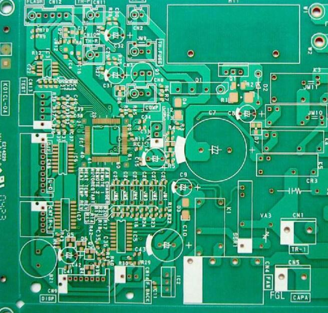
Layout rules of PCB digital-analog hybrid design
Rule 1: Analog devices are placed in the analog area.
Rule 2: Digital devices are laid out in the digital area.
Rule 3: The digital-analog hybrid chip is treated as an analog device and placed in the analog area, but the digital interface needs to be placed close to the corresponding digital device.
Rule 4: Use shielding boxes to protect the following circuits as much as possible
1. The receiving front-end circuit, including the filter, LNA, impedance matching circuit, etc. between the antenna and the receiving chip.
2. Frequency source circuit: VCO, phase locked loop chip, loop filter, crystal oscillator and other PCB circuits.
3. Power amplifier circuit. In the layout, as far as possible, different circuits have independent power supply paths
Rule 5: Place the filter capacitor before the power supply enters the analog area
Rule 6: Digital power and analog power supply power from different directions.
Rule 7: The power supply path in the same direction uses the path from large signal to small signal for power supply.
As shown in the figure: the large-to-small power supply path can reduce the interference of large-signal circuits on small-signal circuits.

Rule 8: The power line of the power amplifier should be as short as possible to reduce the line voltage drop.
Earlier mobile phone battery connectors are generally designed in the middle of the mobile phone board. The upper part is the radio frequency circuit, and the lower part is the digital circuit, as shown in the figure:
The advantage of this layout is that the RF and digital power supply paths are independent, and the power supply path for the attack and amplifier is short.
Rule 9: During the layout and wiring of power modules, reserve copper area for heat dissipation according to power consumption.
Rule 10: Layout is to reserve space for ground vias for important pins.
The ground pin of the radio frequency device needs to be grounded nearby and connected to the reference layer of the radio frequency signal. For example, if the second layer is hollowed out, the ground pin must be connected to the third layer nearby.
Rule 11: The filter capacitor is close to the pin of the power module, and the high-frequency filter capacitor is closer to the pin.
Our factory is located in China. For decades, Shenzhen has been known as the world's electronics R&D and manufacturing center. Our factory and website are approved by the Chinese government, so you can skip the middlemen and buy products on our website with confidence. Because we are a direct factory, this is the reason why 100% of our old customers continue to purchase on i PCB.
No minimum requirements
You can order as little as 1 PCB from us. We will not force you to buy things you really don't need to save money.
Free DFM
Before you pay in the most timely manner, all your orders will receive free engineering document review services by our well-trained professional and technical personnel.