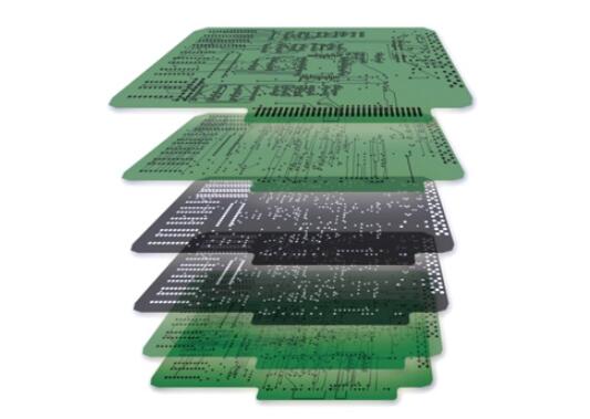
What are the design requirements for multilayer boards pressing structure?
Multilayer PCB is mainly composed of copper foil, prepreg and core board. There are two types of pressing structures, namely, the pressing structure of copper foil and the core board and the pressing structure of the core board and the core board. Preferably, the copper foil and the core board are laminated, and special plates (such as Rogerss 44350, etc.) multilayer boards and mixed-press structure boards can adopt the core board laminated structure. Note that the PCB Construction mentioned here and the stack-up-layers in the drilling diagram are two different concepts. The former refers to the laminated structure when the PCB is laminated, also called the laminated structure, and the latter refers to the stacking sequence of the PCB design, also called the stacking sequence.

1. Design requirements for pressing structure
In order to reduce the warpage of the PCB, the PCB pressing structure should meet the symmetry requirements, that is, the thickness of the copper foil, the type and thickness of the dielectric layer, the pattern distribution type (circuit layer, plane layer), and the vertical pressure relative to the PCB. Centrosymmetric,
2. Conductor copper thickness
(1) The copper thickness of the conductor indicated on the drawing is the finished copper thickness, that is, the outer copper thickness is the thickness of the bottom copper foil plus the thickness of the electroplating layer, and the inner copper thickness is the thickness of the inner bottom copper foil. The outer copper thickness on the drawing is marked as "copper foil thickness + plating, and the inner copper thickness is marked as "copper foil thickness".
(2) Precautions for the application of thick bottom copper at 2OZ and above:
Must be used symmetrically in the entire laminated structure.
Try to avoid placing them on the L2 and Ln-2 layers, that is, the secondary outer layers of the Top and Bottom surfaces, so as to avoid uneven and wrinkled PCB surfaces.
3. Requirements for pressing structure
The pressing process is a key process of PCB manufacturing. The more porous the pressing times, the worse the positioning accuracy of the disc and the more serious the deformation of the PCB, especially when asymmetric pressing. Lamination has requirements for the laminate, such as the copper thickness and the dielectric thickness must match.
iPCB is a high-tech manufacturing enterprise focusing on the development and production of high-precision PCBs. iPCB is happy to be your business partner. Our business goal is to become the most professional prototyping PCB manufacturer in the world. Mainly focus on microwave high frequency PCB, high frequency mixed pressure, ultra-high multi-layer IC testing, from 1+ to 6+ HDI, Anylayer HDI, IC Substrate, IC test board, rigid flexible PCB, ordinary multi-layer FR4 PCB, etc. Products are widely used in industry 4.0, communications, industrial control, digital, power, computers, automobiles, medical, aerospace, instrumentation, Internet of Things and other fields.