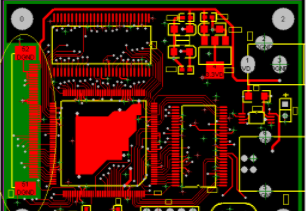
5 basic PCB design specifications you have to see
For many PCB design novices, understanding the most basic specifications of PCB design is the primary task, which will help develop good PCB design habits and be more suitable for all aspects of electronic manufacturing, such as PCB production, SMT chip processing, DIP Plug-ins, etc. The following will introduce the five most basic specifications in PCB design in great detail.
1. Shielding cover design
The distance between the shielding cover and the shielding cover and between the components in the shielding cover and the shielding cover must be greater than 0.4MM
Reason: At present, the width of the shielding cover pad is 0.7MM. In order to reduce the problem of false welding of the shielding cover, especially for models with many shielding covers and mostly special-shaped devices, the corners of the shielding cover are easily welded. At present, the shielding cover is welded. The width of the steel mesh of the plate will be made
0.3MM-0.5MM internal and external reaming treatment

The pad of the shield cover should not be too long, because the pad length is too long and the shield cover is welded with the sawtooth, which will cause local virtual welding. The length of the shielding cover pad is designed to be 2-2.5MM, and the serration height is 0.3MM-0.5MM. For the bending part, it is recommended that the length of the pad is as small as 1.2-1.5MM. The shielding cover pin needs to be made into a serrated shape. Match with the pad.
Reason: The current requirements for shielding cover manufacturers are: the deformation range of 0.1mm is normal, and the deformation position often appears in the bending part. Combined with our current steel mesh thickness of 0.12mm, it is difficult to grasp the welding effect of the pins, and The larger the pad, the less full the amount of solder paste on the pad.
2. The pad spacing between PCB devices
The pad spacing between devices must meet the most basic PCB design requirements.
The distance between the discharge tube and the adjacent component PAD>0.3mm (the distance between the discharge tube and the adjacent component PAD, the same network>0.15mm, different networks>0.2mm) The distance between the discharge tube and the discharge tube>0.1 mm
3. Process clamping edge
The craft edge distance from the top of the veneer>5MM (Note: the machine clamp to the craft edge is 4.5MM) The width of the craft clamping edge>4MM During the PCB mounting process, the PCB should leave a certain edge for easy clamping. Within this range, it is not allowed to place components and pads. In case of high-density boards, the clamping edges can not be left, the process edges can be designed or the panel form can be used. The width depends on the selected SMT equipment. Generally, the process margin is 6.0mm from the top of the component or the edge of the single board, that is, the process margin is closest to the top of the component or >5mm from the PCB inner board.
4. MARK point design
In the design of the MARK points of the PCB board, the MARK points on the same surface are designed to be symmetrical (the left and right MARK points are the same distance from the board edge), and the upper and lower MARK points are asymmetric (the upper and lower MARK points are different from the board edge). Stay dealt with. The diameter of the MARK point on the PCB board is 1.0MM.
5. Positioning hole
The diameter of the positioning hole of the whole panel is 2.5MM+ -0.1MM, and the component is not placed within 1MM around the positioning hole, so as to avoid the sub-board tooling to support the thimble to squeeze the component.
Requirements for positioning holes of the substrates of each panel of the veneer: current standard: 3.0MM-3.8MM
The above are the basic PCB design specifications, which are suitable for beginners and must be mastered and used. In fact, PCB design specifications are far more than these. Designers need to continue to summarize in the complex work, and take manufacturability and clarity as the basic principles to ensure that the PCB design documents sent out are accurate, standardized and clear at a glance. This is also an advanced PCB design. An important aspect of the gap between engineers and beginners.