As the speed increases, EMI becomes more and more serious and manifests itself in many aspects (such as electromagnetic interference at the interconnection). High-speed devices are particularly sensitive to this. As a result, they will receive high-speed false signals, while low-speed devices Will ignore such false signals.
At the same time, EMI also threatens the safety, reliability and stability of electronic equipment. Therefore, when designing electronic products, PCB design is very important to solve the EMI problem.
Electromagnetic Interference (EMI)
Electromagnetic interference (EMI, Electro MagneTIc Interference) can be divided into radiation and conduction interference. Radiated interference means that the interference source uses space as a medium to interfere with its signal to another electrical network. Conducted interference is the use of conductive media as a medium to interfere with signals on one electrical network to another electrical network. In high-speed system design, integrated circuit pins, high-frequency signal lines and various plugs are common sources of radiation interference in PCB board design. The electromagnetic waves they emit are electromagnetic interference (EMI), which will affect themselves and other systems. normal work.

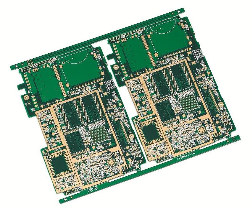
PCB board design skills for EMI
1. Common mode EMI interference source (such as the voltage drop formed by the transient voltage formed on the power bus bar at both ends of the inductance of the decoupling path)
Using low-value inductors in the power layer reduces the transient signals synthesized by the inductors and reduces common-mode EMI.
Reduce the length of the wiring from the power plane to the IC power pin.
Use 3-6 mil PCB layer spacing and FR4 dielectric material.
2. Reduce the loop
Each loop is equivalent to an antenna, so we need to minimize the number of loops, the area of the loop and the antenna effect of the loop. Ensure that the signal has only one loop path at any two points, avoid artificial loops, and try to use the power layer.
3. Filter
Filtering can be used to reduce EMI both on the power line and on the signal line. There are three methods: decoupling capacitors, EMI filters, and magnetic components. EMI filter.
4. Electromagnetic shielding
Try to put the signal traces on the same PCB layer and close to the power layer or ground layer.
The power plane should be as close as possible to the ground plane
5. Layout of parts (different PCB layout will affect the interference and anti-interference performance of the circuit)
Perform block processing according to different functions in the circuit (such as demodulation circuit, high-frequency amplifying circuit and mixing circuit, etc.). In this process, the strong and weak electrical signals are separated, and the digital and analog signal circuits must be separated.
The filter network of each part of the circuit must be connected nearby, which can not only reduce the radiation, but also improve the anti-interference ability of the circuit and reduce the chance of interference.
The parts that are susceptible to interference should be arranged to avoid interference sources, such as the interference of the CPU on the data processing board.
6. Wiring considerations (unreasonable wiring will cause cross interference between signal lines)
There should be no traces close to the frame of the PCB board to avoid disconnection during production.
The power line should be wide, so the loop resistance will be reduced.
The signal line should be as short as possible and the number of vias should be reduced.
The corner wiring cannot use the right-angle method, and the 135° angle is better.
The digital circuit and the analog circuit should be isolated by the ground wire, and the digital ground wire and the analog ground wire should be separated, and finally connected to the power ground.
7. Increase the dielectric constant of the PCB board / increase the thickness of the PCB board
Increasing the dielectric constant of the PCB board can prevent high-frequency parts such as the transmission line close to the board from radiating outward; increasing the thickness of the PCB board and minimizing the thickness of the microstrip line can prevent the electromagnetic wire from overflowing, and also can prevent radiation.