To make a good PCB board, what are the issues to consider?
1. Clear requirements for plate, plate thickness, copper thickness, process, solder mask/character color, etc.
These points are the basis for making a board, so R&D engineers must write clearly. According to the customers I have contacted, Gree has done a relatively good job. The technical requirements of each document are written very clearly, even in normal times. We believe that the most normal use of green solder mask ink and white characters are written in the technical requirements, but some customers can avoid it if they can avoid it. If nothing is written, they will be sent to the manufacturer for proofing, especially some manufacturers have some special requirements. None of them were written out. The first thing the manufacturer had to do after receiving the e-mail was to consult the requirements in this regard, or some PCB manufacturers did not meet the requirements in the end.
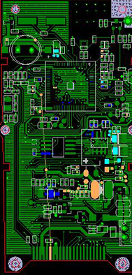
2. Design of drilling
The most direct and biggest problem is the design of the smallest aperture. Generally, the smallest aperture in the board is the aperture of the via. This is directly reflected in the cost. The vias of some boards can obviously be designed as 0.50MM holes, namely Only put 0.30MM, so the cost will directly rise sharply, the manufacturer will increase the price if the cost is high; in addition, there are too many vias, and the vias on some DVDs and digital photo frames are really full. 1000 holes. I have done too many boards in this area. I think it should be 500-600 holes. Of course, some people will say that multiple holes are good for the signal conduction of the board and the heat dissipation. I think this needs a balance., While controlling these aspects, it will not lead to an increase in costs. I can give an example here: our company has a customer who makes DVDs in Shenzhen, and the quantity is very large. This was also the case when we first cooperated. Later, the cost was a big problem for both parties. After communicating with R&D, the aperture of the vias was increased as much as possible, and some vias on the large copper skin were deleted. For example, the heat dissipation hole in the middle of the main IC uses 4 3.00mm holes. Instead, in this way, the cost of drilling is reduced, one square can reduce the drilling cost of tens of dollars, which is a win-win situation for both parties; the other is some slots, such as 1.00MM X 1.20MM Ultra-short slot holes are really very difficult for manufacturers to make. First, it is difficult to control tolerances. The second drill also comes with grooves that are not straight, and some are curved. We have done some of these boards before. As a result, the board with a few cents of renminbi, due to the unqualified slot hole, deducted 1 US dollar/block, we also communicated with the customer about this problem, and later directly switched to the 1.20mm round hole.
3. Circuit design
For line width and line spacing, open circuit and short circuit, etc., they are the most common among manufacturers. Aside from the special ones, for some more conventional boards, I think that the line width and line spacing are of course the larger the better. I have seen some documents, one of them could have been Straight line, there must be a few bends in the middle, there are several lines of the same width and size in the same row, and the spacing is different. For example, the spacing is only 0.10MM in some places, and 0.20MM in some places. I think R&D is in When wiring, pay attention to these details; there are also some circuit pads or traces and the distance between the large copper skin is only 0.127MM, which increases the difficulty of the manufacturer to deal with the film. It is best to have the distance between the pad trace and the large copper skin. 0.25MM or more; some traces have a small safety distance from the periphery or V-CUT, and it is okay for the manufacturer to move them, while others must be done with a good R&D design, and there are even traces that are not connected to the same network., And some are obviously on the same network, but they are not connected. In the end, the manufacturer communicated with R&D and found that it was a short-circuit and open-circuit, and then it was necessary to revise the data. This situation is not rare. Experienced engineers may be able to see For those with inexperience, only follow the design documents. As a result, either modify the document to re-proof or use a blade to scrape or fly the line. For boards with impedance requirements on the circuit, some R&Ds are not written, and in the end it does not meet the requirements. In addition, the through holes of some boards are designed on the SMD PAD, and the tin leaks when soldering.

4. Design of solder mask
The problems that are more likely to occur in solder mask are some copper skins or traces where copper should be exposed. For example, a solder mask should be opened on the copper skin to facilitate heat dissipation, or copper should be exposed on some high-current traces. Generally, these additional solder masks are placed on the Soldermask layer, but for some R&Ds, a new layer is created., On the mechanical layer, on the forbidden wiring layer, there are all kinds of things, not to mention, without special instructions, it is difficult for people to understand. I think the most ideal is to put on the TOP Soldermask or BOTTOMSoldermasK layer is the best, which is the easiest to understand. In addition, it is necessary to explain whether the green oil bridge in the middle of the IC should be retained, and it is best to give an explanation.
5. Character design
The most important aspect of characters is the design requirements of character width and character height. Some boards are not very good in this aspect. The same component even has several character sizes. As a manufacturer, I think it is unsightly. I think I must learn from those motherboard manufacturers., The component characters in rows, the same size, make people look pleasing to the eye. In fact, it’s better to design the characters above 0.80*0.15MM, and the silk screen printing process is better for manufacturers; the other is some large white oil blocks, such as those on the crystal oscillator, or some power strips. Some PCB manufacturers use white oil. Cover the pads, some have to expose the pads, these must also be explained; I have also encountered some wrong silk screen positions, such as swapping the characters of the resistor and the capacitor, but these errors are still very few; The signs that need to be added, such as UL mark, ROHS word, PB mark, manufacturer's LOGO and serial number.
6. Appearance design
Nowadays, the boards are rarely rectangular or the like, and they are all irregular, but mainly there are several kinds of line drawing outlines, which make people unable to choose. In addition, in order to improve the utilization rate of the equipment (such as SMT), V-CUT must be made up, but the board pitches are different. Some have pitch and some have no pitch. It is okay for the first PCB factory to make samples in batches. It will be more troublesome if you have to change suppliers later. The PCB factory does not follow the first factory to fight, the steel mesh will not fit. Therefore, under no special circumstances, it is best not to have spacing; in addition, some file designs may draw a small rectangular hole on the outline layer for the slot to be drilled. This situation is more common in files designed by PROTEL software. Relatively speaking, PADS is better. It is easy to be misunderstood by manufacturers to punch out this hole or make it into NPTH attribute if it is placed on the shape layer. For some PTH attributes, it is easy to cause problems.