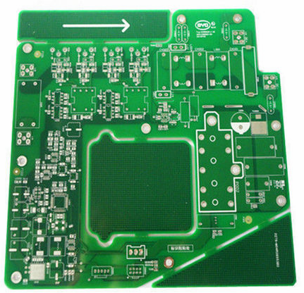
In the PCB design process, if we can predict possible risks in advance and avoid them first, the success rate of PCB design will be greatly improved.
The key to improving the success rate of a board is the signal integrity design. There are many product solutions for current electronic system design, and chip manufacturers have already completed them, including what chips to use, how to build peripheral circuits, and so on. In many cases, hardware engineers hardly need to consider the circuit principle, and only need to make the PCB by themselves.
But it is in the PCB design process that many companies have encountered difficulties, either the PCB design is unstable or it does not work. For large enterprises, many chip manufacturers will provide technical support and guide PCB design. However, it is difficult for some SMEs to get support in this regard. Therefore, you must find a way to complete it yourself, so many problems arise, and it may take several editions and a long time to debug. In fact, if you understand the design method of the system, these can be completely avoided.
Next, let’s talk about techniques to reduce PCB design risks
It is best to consider signal integrity in the system planning stage. The entire system is built like this. Can the signal be received correctly from one PCB to another? This needs to be evaluated in the early stage, and it is not very difficult to evaluate this problem. With a little knowledge of signal integrity, you can do it with a little simple software operation.

In the PCB design process, use simulation software to evaluate specific traces and observe whether the signal quality can meet the requirements. The simulation process itself is very simple. The key is to understand the principle of signal integrity and use it for guidance.
In the process of making PCB, risk control must be carried out. There are many problems that the simulation software has not yet solved, and the designer must control it. The key to this step is to understand where there are risks and how to avoid them. What is needed is knowledge of signal integrity.
After the PCB goes through the automatic tin furnace
The insulating green paint of the circuit under the board will peel off.
What are the reasons?
What is the reason for S/M Peeling after the chemical?
There are three greater possibilities for the green paint to fall off:
The first is that the nature of the green paint itself is not enough to withstand the test of the tin furnace, which may be due to the insufficiency of the green paint due to its expiration or poor operation. The green paint used by the industry is almost always tested for heat resistance and reliability. Therefore, there should be no problems with normality. In this regard, it is necessary to review whether the material itself has changed or the manufacturing process has changed.
The second possibility is the influence of external forces, including flux supply and mechanical collisions, etc., especially in high temperature conditions, the characteristics of green paint are no longer as high as normal temperature environments. At this time, the green paint surface of the circuit board is affected by any external force. Prone to scratches and peeling.
The third greater possibility is that the circuit board bursts due to moisture absorption before the green paint is painted or when it is stored. The volume of water vapor increases nearly three hundred times when heated and vaporized. It is easy to peel off the green paint. This type of problem occurs in the spray tin manufacturing process of the circuit board, and may also occur in the assembly process such as wave soldering and reflow.
There are several possibilities for SMPEELING after chemical gold:
The first possibility is that the treatment in front of copper is not ideal,
The second possibility is insufficient drying before S/M coating.
The third possibility is that the stagnation time is too long to produce an oxide layer,
The fourth possibility is that the material of the green paint itself is not suitable for the chemical gold process.
The fifth possibility is that the degree of polymerization of the green paint is insufficient.
Sixth, if you do more than one high temperature process,
For example: gold plating and gold plating together or twice immersion gold, it may also happen. Because there are many possibilities, you must do a detailed analysis to clarify item by item, but generally speaking, it is very important for the type of S/M.
Some special green paints react slowly to UV light, and require anaerobic and relatively high exposure energy to achieve a high degree of polymerization. If the exposure degree of polymerization is insufficient, the subsequent baking will not be able to fully achieve the desired polymerization strength. If you use such materials, you should clearly inform the operator of the correct handling method, otherwise problems will continue. In addition, if these three points can be grasped well in the PCB design process, then the PCB design risk will be greatly reduced, the probability of error after the board is printed will be much smaller, and the debugging will be relatively easy. Therefore, in the process of making PCB, risk control must be carried out.