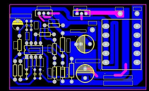
For PCB layout engineers, mobile phones pose the ultimate challenge. Modern mobile phones contain almost all subsystems found in portable devices, and each subsystem has conflicting requirements. A well-designed circuit board must maximize the performance of each device connected to it and avoid interference between multiple systems. The inconsistent requirements of various subsystems will inevitably lead to performance degradation.
Although the audio functionality in mobile phones continues to increase, audio circuits often receive the least attention during the PCB design process.
Mobile phone circuit board design to improve audio performance should:
▪ Carefully consider the underlying planning. The ideal bottom plan should divide different types of circuits into different areas.
▪ Use differential signals as much as possible. Audio devices with differential inputs can suppress noise. It is generally not possible to add a ground wire in the middle of the differential signal. Because the most important point of the application principle of differential signals is to use the benefits of mutual coupling between differential signals, such as magnetic flux elimination and noise immunity.

If you add a ground wire in the middle, it will destroy the coupling effect. There are two points to pay attention to in the layout of the differential pair. One is that the length of the two wires should be as long as possible, and the other is that the distance between the two wires (this distance is determined by the differential impedance) must be kept constant, that is, it must be kept parallel. There are two parallel ways, one is that the two wires run on the same side-by-side, and the other is that the two wires run on two adjacent layers above and below (over-under). Generally, the former has more side-by-side implementations.
▪ Isolate ground current to prevent digital current from adding noise to analog circuits. Basically, it is right to divide and isolate the analog/digital ground. It should be noted that the signal trace should not cross the divided place as much as possible, and the return current path of the power supply and signal should not change too much. The requirement that the digital-analog signal traces cannot cross is because the return current path of the digital signal with a faster speed will flow back to the source of the digital signal along the ground near the bottom of the trace as much as possible. If the digital-analog signal traces cross, the current will be returned. The generated noise will appear in the analog circuit area.
▪ The analog circuit uses star grounding. The current consumption of audio power amplifiers is generally very large, which may have an adverse effect on their own grounding or other reference grounds.
▪ Turn all unused areas on the circuit board into a ground plane. Realize grounding coverage near the signal traces to shunt the excess high-frequency energy in the signal lines to the ground through capacitive coupling.
Mobile phone circuit board design to improve audio performance should not:
▪ Use a hybrid circuit on the board. Although the radio frequency area of a mobile phone is generally considered to be analog, the noise coupled into the audio circuit from the radio frequency area will be demodulated into audible noise.
▪ The analog audio signal wiring is too long. Analog audio traces that are too long may be interfered by noise from digital and RF circuits.
▪ Forget the importance of ground loops. Poorly grounded systems will have serious distortion, noise, crosstalk, and low RF immunity.
▪ Interrupt the natural circuit of digital current. This path produces the smallest loop area, which can reduce antenna influence and inductance effects.
▪ Neglect to place the bypass capacitor as close as possible to the power pin to be bypassed.