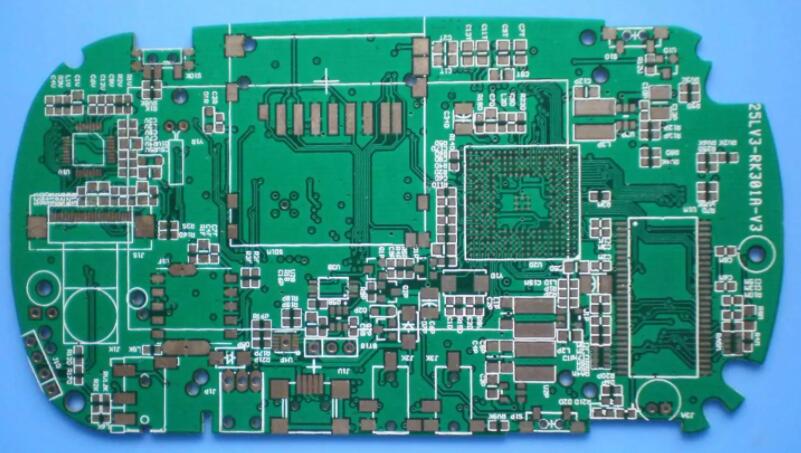
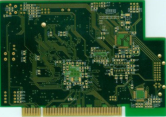
The general PCB design process is as follows: preliminary preparation -> PCB structure design -> PCB layout -> wiring -> wiring optimization and silk printing -> network and DRC inspection and structure inspection -> plate making.
First: Preliminary preparation
1. This includes preparing component libraries and schematics. "If you want to do well, you must first sharpen your tools." To make a good board, in addition to designing the principles, you must also draw well. Before proceeding with PCB design, we must first prepare the schematic SCH component library and PCB component library (this is the first step-very important). The component library can use Protel's own library, but under normal circumstances, it is difficult to find a suitable one. It is best to make your own component library based on the standard size data of the selected device.
In principle, do the PCB component library first, and then do the SCH component library. The PCB component library requirements are high, which directly affects the installation of the board; the SCH component library requirements are relatively loose, as long as you pay attention to the definition of the pin attributes and the corresponding relationship with the PCB components.
PS: Pay attention to the hidden pins in the standard library. After that is the design of the schematic diagram, and when it is done, it is ready to start the PCB design.
2. When making the library of the schematic diagram, pay attention to whether the pins are connected to/output the PCB board and check the library made.
Second: PCB structure design

In this step, according to the determined circuit board plane size and various mechanical positioning, draw the PCB board surface in the PCB design environment, and place the required connectors, buttons/switches, digital tubes, indicator lights, input, and output according to the positioning requirements., Screw holes, assembly holes, etc. and fully consider and determine the wiring area and non-wiring area (such as how much area around the screw hole belongs to the non-wiring area).
(--Special attention is required. When placing components, you must consider the actual size of the components (occupied area and height), the relative position between the components-the space size, the surface on which the components are placed, to ensure the circuit board At the same time, the electrical performance and the feasibility and convenience of production and installation should be properly modified under the premise of ensuring that the above principles can be reflected. It’s placed "scatteredly").
Third: PCB layout
1. Make sure that the schematic diagram is correct before layout-this is very important! -----Very important!
After the schematic diagram is drawn, check items: power supply network, ground network, etc.
2. Pay attention to the surface where the device is placed (especially the plug-in unit, etc.) and the placement method of the device (in-line or vertical placement) to ensure the feasibility and convenience of installation.
3. To put it bluntly, the layout is to put devices on the board. At this time, if all the preparations mentioned above are done, you can generate the netlist (Design->CreateNetlist) on the schematic, and then import the netlist (Design->LoadNets) on the PCB diagram. You can see that the devices are all piled up, and there are flying wires between the pins to indicate the connection, and then you can lay out the devices.
The general layout is carried out according to the following principles:
The side on which the device is placed should be determined during layout: Generally speaking, the patch should be placed on the same side, and the plug-in depends on the specific situation.
1. According to the reasonable division of electrical performance, it is generally divided into: digital circuit area (that is, afraid of interference and interference), analog circuit area (fear of interference), power drive area (interference source);
2. Circuits that complete the same function should be placed as close as possible, and the components should be adjusted to ensure the most concise connection; at the same time, adjust the relative position between the functional blocks to make the connection between the functional blocks the most concise;
3. For high-quality components, the installation location and installation strength should be considered; heating components should be placed separately from temperature-sensitive components, and heat convection measures should be considered when necessary;
4. The I/O drive device should be as close as possible to the edge of the printed board and to the lead-out connector;
5. The clock generator (such as: crystal oscillator or clock oscillator) should be as close as possible to the device that uses the clock;
6. The layout requirements should be balanced, dense and orderly, and not top-heavy or heavy.
Fourth: Wiring
Wiring is the most important process in the entire PCB design. This will directly affect the performance of the PCB board. In the process of PCB design, there are generally three divisions of wiring: First, the layout is the most basic requirement for PCB design. If the lines are not connected and there are flying lines everywhere, it will be a substandard board, and it can be said that you have not yet started. The second is the satisfaction of electrical performance. This is the standard to measure whether a printed circuit board is qualified. This is after the distribution, carefully adjust the wiring to achieve the best electrical performance, and then the aesthetics. If your wiring is properly routed, there is nothing to affect the performance of the electrical appliances, but at first glance it looks messy, plus colorful and colorful, then no matter how good your electrical performance is, it is still a piece of rubbish in the eyes of others. This brings great inconvenience to testing and maintenance. Wiring must be neat and uniform, not criss-cross and unorganized. These must be achieved while ensuring the performance of electrical appliances and meeting other individual requirements, otherwise it will be the last one.
The wiring is mainly carried out according to the following principles:
1. Generally, the power line and ground line should be wired first to ensure the electrical performance of the circuit board. Within the scope permitted by conditions, try to widen the width of the power and ground lines, preferably the ground line is wider than the power line, their relationship is: ground line>power line>signal line, usually the signal line width is: 0.2~0.3mm, The thinnest width can reach 0.05~0.07mm, and the power cord is generally 1.2~2.5mm. For digital circuit PCB, a wide ground wire can be used to form a loop, that is, a ground net can be used (the ground of analog circuit cannot be used in this way );
2. Wire lines with strict requirements (such as high-frequency lines) in advance. The edges of the input end and the output end should be avoided adjacently and parallel to avoid reflection interference. If necessary, grounding should be added, and the wiring of two adjacent layers should be mutually. Vertical and parallel are prone to parasitic coupling;
3. The housing of the oscillator is grounded, and the clock line should be as short as possible and cannot be drawn everywhere. Under the clock oscillation circuit, the area of the special high-speed logic circuit should be enlarged, and other signal lines should not be used to make the surrounding electric field approach zero;
4. Use 45° folded lines as much as possible, and 90° folded lines should not be used to reduce the radiation of high-frequency signals; (the lines with high requirements should also use double arc lines);
5. Do not form a loop in any signal line. If it is unavoidable, the loop should be as small as possible; the signal line's vias should be as few as possible;
6. The key line should be as short and thick as possible, and protective ground should be added on both sides;
7. When transmitting sensitive signals and noise field band signals through flat cables, they should be led out in the way of "ground wire-signal-ground wire";
8. Test points should be reserved for key signals to facilitate debugging, production, maintenance and testing;
9. After the schematic wiring is completed, the wiring should be optimized; at the same time, after the preliminary network inspection and DRC check are correct, the unwiring area is filled with ground wires, and a large area of copper layer is used as the ground wire. The places used are connected to the ground as a ground wire. Or it can be made into a multi-layer board, and the power supply and ground wire occupy one layer each.
Fifth: add teardrops
Sixth: The first item to check, look at Keepout layer, top layer, bottom layer topoverlay, bottomoverlay in turn.
Seventh: electrical rules inspection: vias (0 vias-very incredible; 0.8 dividing line), whether there is a disconnected netlist, minimum spacing (10mil), short circuit (analyze each parameter one by one)
Eighth: Check the power line and the ground wire-interference. (The filter capacitor should be close to the chip)
Ninth: After the PCB is completed, reload the net mark to check whether the netlist has been modified-very effective.
Tenth: After the PCB circuit board is completed, check the lines of the core components to ensure accuracy.