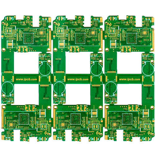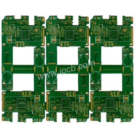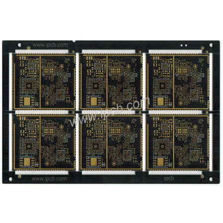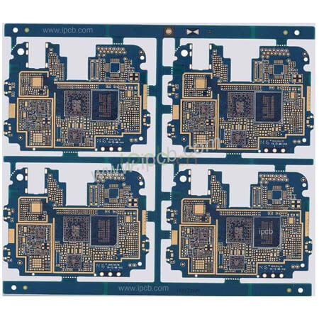
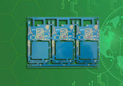

Modelo: teléfono móvil HDI PCB
Capa: 60 capas
Material: Sy s1000 - 2
Construcción: 1 + 4 + 1 HDI de primer orden
Espesor del producto terminado: 0,8 mm
Espesor del Cobre: 0,5 Oz
COLOR: verde / blanco
Tratamiento de superficie: inmersión en oro
Seguimiento / espacio mínimo: 3mil / 3mil
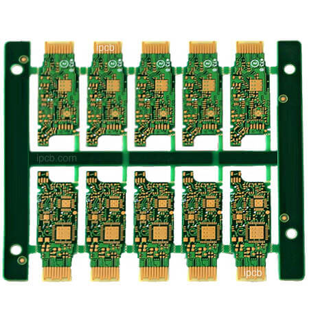
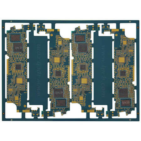
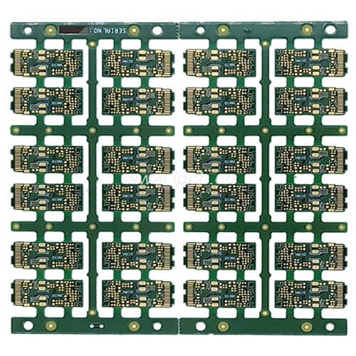
Aplicación: tablero de PCB HDI para teléfonos móviles
Un buen diSeño laminado permite Placa de circuito impreso Mejor rendimiento. En la actualidad, la competencia en el mercado de teléfonos móviles es cada vez más feroz, El costo es sin duda un factor importante para la supervivencia. Es un teléfono de bajo costo. Placa de circuito impreso Seis niveles de primer orden HDI Placa de circuito impreso Board Detección.Producción de productos primarios HDI Placa de circuito impreso Board Es relativamente simple., El proceso y el proceso están bien controlados, Y el costo más bajo.
Leyenda del agujero ciego mecánico de primer orden (la siguiente figura no está diseñada para agujeros superpuestos)

hdi pcb
HDI: abreviatura de interconexión de alta densidad, interconexión de alta densidad, perforación no mecánica, anillos de agujeros micro - ciegos de hasta 6 mils, ancho de cableado entre capas internas y externas. El método de fabricación de placas multicapa con una distancia de alambre inferior a 4 mils y un diámetro de almohadilla inferior a 0,35 MM se llama hdi pcb.
Cómo definir varios niveles de hdi pcb
Agujero ciego: abreviatura de agujero ciego para realizar la conexión y conducción entre la capa interior y la capa exterior.
Paso subterráneo: la abreviatura de paso subterráneo realiza la conexión entre la capa interior y la capa interior, y los agujeros ciegos son más grandes.
El agujero ciego es un pequeño agujero de 0,05 mm ~ 0,15 mm de diámetro. Los agujeros ciegos enterrados se forman mediante perforación láser, grabado plasmático y perforación inducida por la luz. La perforación láser se divide generalmente en CO2 y YAG laser Machine (UV).
La primera y segunda etapa de la placa de PCB de 6 capas se utilizan para la placa de PCB que necesita perforación láser, es decir, la placa de hdi pcb.
6 capas de Placa de circuito impreso HDI de primer orden agujeros ciegos: 1 - 2, 2 - 5, 5 - 6. Es decir, 1 - 2, 5 - 6 requiere perforación láser.
Segundo piso, 6º piso HDI Placa de circuito impreso Board Agujero ciego del dedo: 1 - 2, 2 - 3, 3 - 4, 4 - 5, 5 - 6. Requiere dos perforaciones láser. Primero perforar 3 - 4 agujeros enterrados, then press 2 - 5, Luego practique 2 - 3, Uso inicial de 4 - 5 agujeros láser, Luego presione 1 - 6 por segunda vez, Luego perforar 1 - 2 y 5 - 6 agujeros láser por segunda vez. Finalmente perforar. Como puede ver, el segundo orden HDI Placa de circuito impreso Board Ha sido presionado dos veces, perforado dos veces por láser.
Además, Segundo orden HDI Placa de circuito impreso Board También se divide en: agujero equivocado de segundo orden HDI Placa de circuito impreso Board Agujero apilado de segundo orden HDI Placa de circuito impreso Board. Agujero de error de segundo orden HDI Placa de circuito impreso Board Indica que los agujeros ciegos 1 - 2 y 2 - 3 están entrelazados, Segundo orden HDI Placa de circuito impreso board Agujeros ciegos 1 - 2 y 2 - 3 superpuestos, Ejemplo: ciego: 1 - 3, 3 - 4, 4 - 6. Espera un minuto., Tercer orden, Cuarto orden. Todos son iguales.
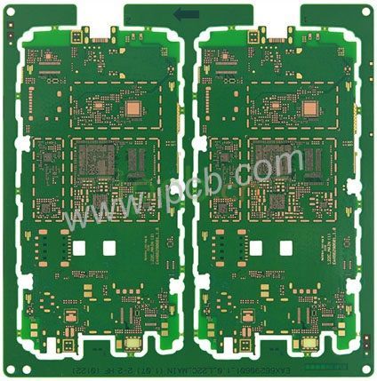
Modelo: teléfono móvil HDI PCB
Capa: 60 capas
Material: Sy s1000 - 2
Construcción: 1 + 4 + 1 HDI de primer orden
Espesor del producto terminado: 0,8 mm
Espesor del Cobre: 0,5 Oz
COLOR: verde / blanco
Tratamiento de superficie: inmersión en oro
Seguimiento / espacio mínimo: 3mil / 3mil
Aplicación: tablero de PCB HDI para teléfonos móviles
For PCB technical problems, iPCB knowledgeable support team is here to help you with every step. You can also request PCB quotation here. Please contact E-mail sales@ipcb.com
We will respond very quickly.