In electronic equipment, grounding is an important method to control interference. If the grounding and shielding can be properly combined and used, most of the interference problems can be solved. The ground structure of electronic equipment roughly includes system ground, chassis ground (shield ground), digital ground (logical ground), and analog ground.
In the design of the ground wire of the PCB board, the grounding technology is applied to both the multilayer PCB and the single-layer PCB. The goal of grounding technology is to minimize the ground impedance, and hence to reduce the potential of the ground loop from the circuit back to the power supply.
(1) Correctly choose single-point grounding and multi-point grounding
In the low-frequency circuit, the working frequency of the signal is less than 1MHz, its wiring and the inductance between the devices have little influence, and the circulating current formed by the grounding circuit has a greater influence on the interference, so one point grounding should be adopted. When the signal operating frequency is greater than 10MHz, the ground wire impedance becomes very large. At this time, the ground wire impedance should be reduced as much as possible, and the nearest multiple points should be used for grounding. When the operating frequency is 1~10MHz, if one-point grounding is used, the length of the ground wire should not exceed 1/20 of the wavelength, otherwise the multi-point grounding method should be used. The high-frequency circuit should be grounded at multiple points in series, the ground wire should be short and thick, and a grid-like large-area grounding copper foil should be arranged around the high-frequency component as much as possible.
(2) Separate the digital circuit from the analog circuit
There are both high-speed logic circuits and linear circuits on the circuit board. They should be separated as much as possible, and the ground wires of the two should not be mixed, and they should be connected to the ground wires of the power supply terminal. Try to increase the grounding area of the linear circuit as much as possible.
(3) Thicken the ground wire as much as possible
If the ground wire is very thin, the ground potential will change with the current change, causing the timing signal level of the electronic device to be unstable and the anti-noise performance to deteriorate. Therefore, the ground wire should be as thick as possible so that it can pass three times the allowable current of the printed circuit board. If possible, the width of the ground wire should be greater than 3mm.
(4) Form the ground wire into a closed loop
When designing the ground wire system of the printed circuit board composed of only digital circuits, making the ground wire into a closed loop can significantly improve the anti-noise ability. The reason is that there are many integrated circuit components on the printed circuit board, especially when there are components that consume more power, due to the limitation of the thickness of the ground wire, a large potential difference will be generated on the ground junction, which will cause the anti-noise ability to decrease, If the grounding structure is formed into a loop, the potential difference will be reduced and the anti-noise ability of electronic equipment will be improved.

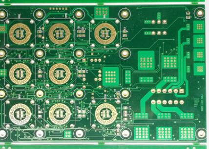
(5) When adopting the multi-layer circuit board design, one of the layers can be used as the "all ground plane", which can reduce the grounding impedance and at the same time play a shielding role. We often place a wide ground wire around the printed board, which also plays the same role.
(6) Ground wire of single-layer PCB
In a single-layer (single-sided) PCB, the width of the ground wire should be as wide as possible, and should be at least 1.5mm (60mil). Since star wiring cannot be implemented on a single-layer PCB, the change in jumper and ground wire width should be kept to a minimum, otherwise it will cause changes in line impedance and inductance.
(7) Ground wire of double-layer PCB
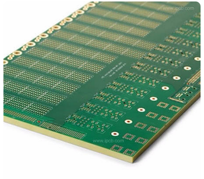
In double-layer (double-sided) PCBs, ground grid/dot matrix wiring is preferred for digital circuits. This wiring method can reduce ground impedance, ground loops, and signal loops. As in a single-layer PCB, the width of the ground and power lines should be at least 1.5mm.
Another layout is to put the ground plane on one side and the signal and power lines on the other side. In this arrangement, the ground loop and impedance will be further reduced. At this time, the decoupling capacitor can be placed as close as possible between the IC power supply line and the ground plane.
(8) PCB capacitance
On a multilayer board, the PCB capacitance is generated by the thin insulating layer separating the power plane and the ground. On a single-layer board, the parallel arrangement of power lines and ground lines will also have this capacitive effect. One advantage of the PCB capacitor is that it has a very high frequency response and low series inductance evenly distributed across the entire surface or the entire line. It is equivalent to a decoupling capacitor uniformly distributed across the entire board. No single discrete component has this feature.
(9) High-speed circuit and low-speed circuit
High-speed circuits and components should be placed closer to the ground plane, and low-speed circuits and components should be placed closer to the power plane.
(10) Copper filling of ground
In some analog circuits, the unused circuit board area is covered by a large ground plane to provide shielding and increase decoupling capabilities. But if this copper area is suspended (for example, it is not connected to the ground), then it may behave as an antenna and will cause electromagnetic compatibility problems.
(11) Ground plane and power plane in multilayer PCB
In a multi-layer PCB, it is recommended to place the power plane and the ground plane as close as possible to adjacent layers in order to generate a large PCB capacitance on the entire board. The fastest critical signals should be close to one side of the ground plane, and non-critical signals should be placed close to the power plane.
(12) Power requirements
When the circuit requires more than one power supply, use grounding to separate each power supply. But it is impossible to ground multiple points in a single-layer PCB. One solution is to separate the power cord and ground wire from one power supply from other power cords and ground wires, which also helps to avoid noise coupling between power supplies.