This application note provides guidance and advice on the design and layout of radio frequency (RF) printed circuit boards(PCBS), including some discussions on mixed-signal applications, such as digital, analog, and RF components on the same PCB. The content is organized by topic and provides "practice" guidelines that should be applied in conjunction with all other design and manufacturing guidelines that may be applicable to specific components, PCB manufacturers, and materials.

Radio frequency transmission line
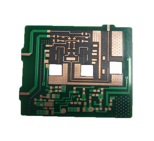
Many Maxim RF components require impution-controlled transmission lines to transmit RF power to (or from) an IC pin on the PCB. These transmission lines can be implemented in the outer layer (top or bottom layer) or buried in the inner layer. Guides to these transmission lines include discussions of microstrip lines, ribbon lines, coplanar waveguides (ground), and characteristic impedances. It also introduces transmission line bend Angle compensation and transmission line layer change.

The microstrip line
This type of transmission line consists of a fixed-width metal wire (conductor) and a ground area directly below (adjacent layer). For example, wiring on layer 1 (top metal) requires a solid ground zone on layer 2 (Figure 1). The width of the wiring, the thickness of the dielectric layer, and the type of dielectric determine the characteristic impedance (usually 50 or 75 ω).
stripline
The wire comprises an inner layer of fixed width wiring, and a ground area above and below. The conductor may be in the middle of the ground zone (Figure 2) or have a certain offset (Figure 3). This method is suitable for rf wiring in the inner layer.
Coplanar waveguide (grounded)
Coplanar waveguides provide better isolation between adjacent RF lines and between other signal lines (end view). The medium includes an intermediate conductor and a ground region on both sides and below (FIG. 4).

It is recommended to install "fences" through holes on both sides of the coplanar waveguide. This top view provides an example of installing a row of ground through holes in the top metal ground zone on each side of the middle conductor. The loop current from the top layer is short-circuited to the ground below.
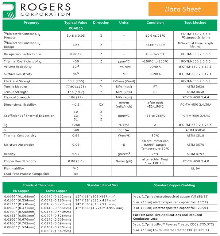
There are a variety of calculation tools for characteristic impedance (Lao Wu recommended using the impedance calculation tool) that can be used to correctly set the line width of the signal conductor to achieve the target impedance. However, care should be taken when entering the dielectric constant of the board layer. The outer substrate layer of a typical PCB contains less glass fiber composition than the inner layer, so the dielectric constant is lower. For example, the dielectric constant of FR4 materials is generally εR = 4.2, while the outer substrate (semi-cured plate) layer is generally εR = 3.8. The example below is for reference only, with a metal thickness of 1oz copper (1.4 mils, 0.036mm).