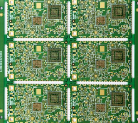
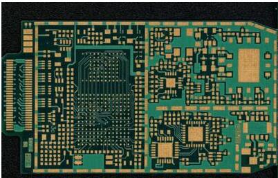
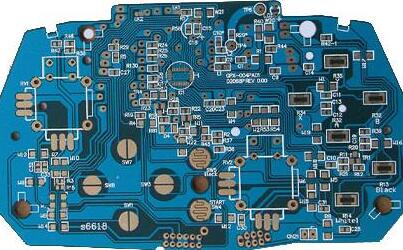
The electroplating of high-aspect-ratio through holes is a key in the manufacturing process of multi-layer PCB boards. Since the ratio of the board thickness to the aperture is 5:1 higher, it is difficult to make the copper plating layer uniformly cover the entire hole wall. very big. Due to the small aperture and high depth, it is difficult for the through hole to meet the process requirements during the entire process. The most prone to quality problem is the removal of epoxy drilling dirt, ie etchback, which makes it difficult to control the microetching depth of etchback, because the pore size is small and it is difficult for the deep pit etching liquid to pass through the entire hole smoothly, and some first contact The etched part of the epoxy resin is etched. When it is completely immersed in the etched liquid, the etched depth of the earlier part exceeds the standard, exposing the glass fiber.
The formation of voids makes the subsequent copper sinking unable to cover all, and voids will appear. The second is that during the copper sinking process, the exchange of the solution is blocked, and it is very difficult to replace the fresh copper sinking solution, which greatly reduces the coverage of the copper sinking. The third is that the dispersing ability of electroplating does not meet the process requirements, and it is easy to dissolve a part of the copper immersion layer, forming voids or no copper plating layer. In this case, how to use the existing process equipment to improve the reliability of plated holes and the complete compliance of the hole plating is the focus of this article.
1. Analysis on the Causes of Defects in High Aspect Ratio Through Hole Plating
In order to ensure the high reliability and high stability of the quality of the multilayer PCB board, it is necessary to fully understand the key control points in the whole process of the multilayer PCB board manufacturing. To be more specific is the process that is prone to quality problems. It is not only necessary to know the location where the problem occurs, but also the root cause of the defect and the factors that directly affect it. Through years of production experience in the production of multi-layer PCB boards, the part where quality problems often occur is to remove epoxy drilling (ie, etchback). why? Because this type of multi-layer PCB board is thick and has a small and deep hole diameter, it is difficult for the etching liquid to pass through the entire hole smoothly. In order to make the tap water flow smoothly. Also, since the flow of the pore solution flows into the hole by its own strength, if there is no pressure, it will completely flow through the hole wall. At the same time, the resin itself has the repulsive force of water, which makes it more difficult to pass through the entire hole. Some epoxy resin parts that are in contact first are etched, and when they are completely immersed in the etch solution, the depth of the etched portion of the first part exceeds the standard, exposing the glass fiber and forming a cavity so that the later copper can not cover all of it.
Hollow phenomenon appears. In the process of copper sinking, the fluidity of the solution in the hole is poor. The main reason is that the hole diameter is small, the hole is deep and the resistance to the solution on both sides of the hole is too large, so that the reacted solution in the hole cannot be replaced with fresh copper sinking solution in time, The part that lacks copper ions but is copper-immersed will also be eroded by the solution. In addition, after cleaning the boards treated with other treatment solutions, the water in the holes is not exhausted, and air bubbles are formed when the copper sink is carried out, which hinders the reduction of copper ions and there will be a lack of conductive layer in this part. During electroplating, due to the limited dispersion ability of bright acid copper plating, it is difficult for the current to reach the central part when an impulse current is applied. It is often due to incomplete copper deposition, and the part where the copper has been sinked is not in place due to the current. Obtain the deposited layer, which is eroded and dissolved by the acid solution, forming a cavity. If the impulse current is too large, the parts where the copper has been sinked, especially the two ends of the orifice, will be ablated.

2. Control and Countermeasures of High Aspect Ratio Through Hole Plating
According to the analysis of the reasons discussed above, for the actual situation of copper sinking and electroplating of high aspect ratio multilayer PCB boards, corresponding process countermeasures must be taken to strengthen key control for the most problematic parts. Especially when performing epoxy drilling, on the one hand, it is necessary to choose an etchback solution with good wetting performance; on the other hand, a horizontal vibration device is adopted to enable the etchback solution to pass through the entire hole smoothly, so that the formed after treatment The bubbles are driven away, and the loose epoxy resin that has been swelled is removed from the surface of the inner copper ring, presenting an ideal metallic luster, and increasing the bonding force with the copper sink layer and the electroplating layer.
Because the inner circuit of the multi-layer PCB board depends on the complete hole plating layer to achieve reliable electrical interconnection with the outer layer or the required inner layer, if the hole plating layer is disconnected from the inner layer circuit or the connection is severely defective, it will After assembly, the circuit is completely broken. If the inner layer of epoxy stain is not firmly adhered to the hole wall, that is, the copper layer is plated with poor bonding holes, and it will fall off due to thermal shock during electrical installation or will be released during a pull-off test. . Therefore, improving the etchback process method, increasing the flow of etchback fluid in the hole, constantly replacing fresh etchback fluid, and ensuring that the epoxy drilling dirt of the inner copper ring is clean is the basis for ensuring the integrity of the plating layer in the hole.
In the second aspect, to solve the quality problem of sinking copper, it is necessary to analyze the key points of sinking copper for small holes and hole depth. The important thing is to ensure that the copper sinking solution flows smoothly in the hole and constantly replace it so that the copper sinking will form a dense conductive layer on the surface of the hole wall. The specific method is based on the characteristics of the thickness and aperture ratio of the multi-layer PCB board. In addition to choosing the more active copper-immersed series, the formula and process conditions are relatively wide, and the main reason is to increase the fluidity of the small hole solution.
For the auxiliary equipment of the Plating Hole, a vibration device should be added in the key process of the plated hole. The purpose is to escape the air bubbles in all the holes on the multilayer PCB board, and more importantly, to ensure the free flow of the copper sinking liquid in the hole., It can fully contact with the hole wall to complete the reaction, and the deposited layer is intact and defect-free. However, it is also extremely important to consider how to match the mounting method of this device. If a basket frame is used to mount the copper sinker, the plate must be tilted at an angle, and a swing device can be added to improve the fluidity of the copper sinker in the hole.