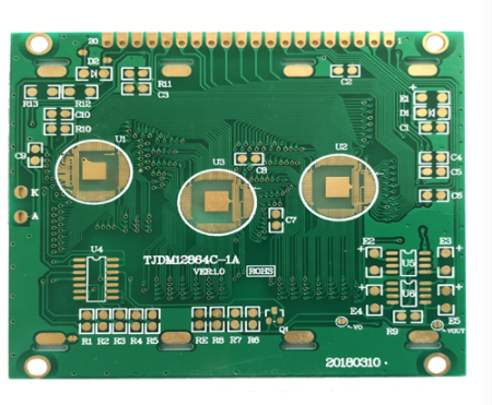
What are the reasons why the circuit board wrinkles and blisters in the soldering ink
The blistering of the circuit board surface is actually a problem of poor board bonding, that is, the surface quality of the board, which contains two aspects:
1. The cleanliness of the circuit board surface;
2. The problem of surface micro-roughness (or surface energy). The blistering problems on the PCB surface of all circuit boards can be summarized as the above-mentioned reasons. The bonding force between the plating layers is poor or too low, and it is difficult to resist the plating stress, mechanical stress and thermal stress generated during the production and processing of the circuit board in the subsequent PCB circuit board production and assembly process, and finally cause the difference between the plating layers Degree of separation phenomenon.
Some factors that may cause poor board quality in the production and processing process are summarized as follows:
1. The problem of substrate processing: especially for some thinner substrates (generally below 0.8mm), because the rigidity of the substrate is poor, it is not suitable to use a brushing machine to brush the plate. This may not be able to effectively remove the protective layer specially treated to prevent the oxidation of the copper foil on the board surface during the production and processing of the substrate. Although the layer is thin and the brush is easier to remove, it is more difficult to use chemical treatment, so in production It is important to pay attention to control during processing, so as to avoid the problem of blistering on the board caused by poor bonding between the copper foil of the board substrate and the chemical copper; this problem will also cause blackening and browning when the thin inner layer is blackened. Poor, uneven color, partial black browning and other problems.

2. The phenomenon of poor surface treatment caused by oil stains or other liquids contaminated with dust during machining (drilling, lamination, milling, etc.) of the circuit board surface.
3. Water washing problem: the electroplating treatment of copper deposits has to go through a lot of chemical treatments. There are many chemical solvents such as acid and alkali, electrodeless organic and so on. The surface of the circuit board is not clean with water, especially the adjusted degreasing agent for copper deposits, which will not only cause Cross-contamination will also cause poor local treatment of the board surface or poor treatment effect, uneven defects, and cause some bonding problems; therefore, it is necessary to strengthen the control of washing, mainly including the flow of washing water, water quality, The washing time and the dripping time of the panels are controlled; especially in winter, the temperature is lower, the washing effect will be greatly reduced, and more attention should be paid to the strong control of the washing;
4. Poor sinking copper brush plate: the pressure of the sinking copper front grinding plate is too large, causing the orifice to be deformed, brushing out the copper foil rounded corners of the orifice or even leaking the substrate, which will cause the sinking copper electroplating, spraying and soldering, etc. Foaming phenomenon at the orifice; even if the brush plate does not cause leakage of the substrate, the excessively heavy brush plate will increase the roughness of the orifice copper, so the copper foil at this place is likely to be over-roughened during the micro-etching roughening process, There will also be certain quality hidden dangers; therefore, it is necessary to strengthen the control of the brushing process, and the brushing process parameters can be adjusted to the best through the wear scar test and the water film test;
5. Micro-etching in the pre-treatment of copper sinking and the pre-treatment of pattern plating: Excessive micro-etching will cause the hole to leak the base material and cause blistering around the orifice; insufficient micro-etching will also cause insufficient bonding force and cause blistering. ; Therefore, it is necessary to strengthen the control of micro-etching; generally the depth of micro-etching before copper sinking is 1.5-2 microns, and the micro-etching before pattern electroplating is 0.3-1 microns. If possible, it is best to pass chemical analysis and simple test weighing method. Control the thickness of the microetching or the etching rate; under normal circumstances, the surface of the microetched plate is bright, uniform pink, without reflection; if the color is uneven, or there is reflection, it means that there is a hidden quality problem in the pre-processing of the process; pay attention to strengthen the inspection; in addition, The copper content of the micro-etching tank, the temperature of the bath, the loading amount, and the content of the micro-etching agent are all items to be paid attention to;
6. Poor rework of copper sinking: some copper sinking or reworked boards after pattern transfer may cause blistering on the board surface due to poor fading, improper rework methods or improper control of the micro-etching time during the rework process or other reasons; If copper plate rework is found to be bad on the line, you can directly remove the oil from the line after washing with water and then directly rework without corrosion after pickling; it is best not to re-degrease or micro-etch; for the boards that have been electrically thickened by the circuit board., Should the micro-etching tank be deplated now, pay attention to the time control, you can use one or two plates to roughly measure the deplating time to ensure the deplating effect; after the deplating is completed, apply a set of soft brushes and then press The normal production process is to sink copper, but the corrosion and micro-etching time should be halved or necessary adjustments;