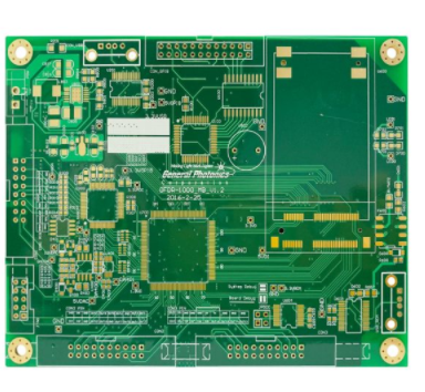
The whole process of manual PCB patch production that PCB Xiaobai must know
Time flies, and I unknowingly I have been dealing with the electronics industry for 3 years. From a little white who basically doesn’t know much about electronic components, to now being able to design circuit boards individually, the road I have traveled over the years is Personally feel so bumpy and bitter! I remember that when I first touched the PCB board soldering (PCB patch/SMT processing), I soldered quite a lot of PCB circuit boards, especially the small chip exclusion. I soldered several times and the pads were all Almost everything I made was useless, and the electronic components of the plug-in were also soldered off a lot of pads by me. All in all, I, like other novices in the industry, have an unsightly past. But when the number of circuit board soldering began to increase, gradually, nowadays almost no pads will be dropped.

Real knowledge comes out of practice, maybe it's just such a personal truth. At least it applies to me!
However, I guess that many of my colleagues who are new to circuit board design should be exactly the same as me many years ago. Soldering is really a difficult bone (of course, it can’t be said to be too absolute, there will still be great gods). It’s just that today’s rookie is not here to discuss the level of soldering process with the big guys, but want to briefly introduce to the big guys a quicker and more economical and practical PCB board soldering technology. The PCB patch is basically like this. Work flow:
1. Open steel mesh
2. Brush solder paste
3. Paste components
4. Over welding machine
5. To be tested
The method steps introduced above are mainly applicable to PCB circuit boards with many electronic components on the PCB board. Those who are soldering mainstream plug-in components should not use the above methods.
The first step is to open a steel mesh when making the circuit board. Speaking of this open steel mesh, as far as I know, there are different prices. For example, there are ordinary corroded steel meshes and laser ones. Considering the price factor, the laser is of course much more expensive. For example, the double-sided stencil I opened is only about 70, but the laser stencil is about 200. I haven't used a laser yet, and I can't say what advantages it has, but the corrosion effect seems to be quite good.
In addition to the steel mesh, the stainless steel shelf on which the steel mesh is placed is also indispensable. This is a stainless steel shelf around Ben Xiaobai:
Next, fix the position of the steel mesh with a steel mesh frame
After placing the stencil correctly, put the circuit board in immediately. After that, we must pay attention to manually adjust the specific position of the circuit board, so that the pad is aligned with the position of the hole on the stencil. After the position of the hole is aligned, the next step is to brush the solder paste. Pour the solder paste on the stencil, and use a flat blade to evenly distribute the solder paste on the pad aperture (observe whether there is any part that is not brushed)
After the solder paste is brushed, we need to carefully paste the electronic components one by one with the camera. After the electronic components are all glued in place, we can place the circuit board in the reflow soldering machine for soldering.
The circuit board is all soldered to the board by the reflow soldering machine. As shown in the enumerated picture, how is this effect? At least it is much more exquisite than hand-soldered. In addition, it is necessary to conduct quality inspections and instrumental inspections artificially, and this is the real end.
The above are some of my experience. The general steps about PCB placement are here. Friends who want to practice can give it a try.