In the electronics industry, there is a key component called PCB (PrintedCircuitBoard), the Chinese name is printed circuit board). This is a basic component, which makes it difficult for many people to explain what a PCB is. This article will explain the composition of PCB in detail, as well as some commonly used terms in the field of PCB.
In the next few pages, we will discuss the composition of PCB proofing, circuit board factories, and circuit board factories, including some terminology, a brief assembly method, and an introduction to the PCB design process.
PCB (PrintedCircuitBoard) is the most common name, and it can also be called "printedwiringboards" or "printedwiringcards". Before the advent of the PCB, the circuit was composed of point-to-point wiring. The reliability of this method is very low, because as the circuit ages, the rupture of the circuit will cause the circuit node to open or short circuit.
As the electronics industry develops from vacuum tubes and relays to silicon semiconductors and integrated circuits, the size of electronic components has decreased and the prices have also fallen. Electronic products appear more and more frequently in the consumer field, prompting manufacturers to find smaller and more cost-effective solutions. Thus, the PCB was born.
PCB looks like a multi-layer cake or lasagna – layers of different materials are pressed together by heat and adhesive.

Let's start from the middle level.
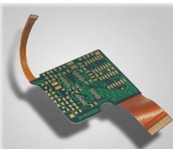
The substrate of PCB is generally glass fiber. In most cases, the glass fiber substrate of PCB generally refers to the material "FR4". The solid material "FR4" is a fiberglass board, which gives the PCB hardness and thickness. In addition to the FR4 fiberglass board, there are flexible circuit boards produced on flexible high-temperature plastics (polyimide or similar) and so on.
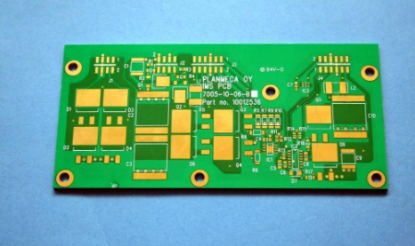
You may find PCB boards of different thicknesses; however, the thickness of Shenzhen Zhongke Circuits products is mostly 1.6mm. Some products in other electronics industries also use other thicknesses, which are all arranged according to the customer's product requirements.
Inexpensive PCBs and hole boards are made of materials such as epoxy resin or phenol, which lack the durability of FR4 fiberglass board, but are much cheaper. When soldering things on this kind of circuit board, you will smell a lot of peculiar smell. This type of substrate is often used in very low-end consumer products. Phenolic substances have a low thermal decomposition temperature, too long welding time will cause them to decompose and carbonize, and emit an unpleasant smell.
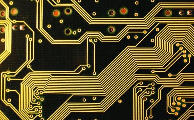
The next introduction is a very thin layer of copper foil, which is pressed onto the substrate through heat and adhesive during production. On a double-sided circuit board, the copper foil will be pressed to the front and back sides of the substrate. In some low-cost occasions, copper foil may only be pressed on one side of the substrate. When we refer to "double-sided board" or "two-layer board", we mean that there are two layers of copper foil on our lasagna. Of course, in different PCB circuit board designs, the number of copper foil layers may be as few as one layer, or more than 16 layers.
There are many types of thickness of the copper layer of the PCB circuit board, and it is expressed in terms of weight. Generally, the weight (oz. oz) of the copper evenly covering one square foot is used. The copper thickness of most PCBs is 1oz (1oz=35um), but some high-power PCB circuit boards may use 2oz or 3oz copper thickness. Converting ounces (oz) per square foot, it is about 35um or 1.4mil copper thickness.
Above the copper layer is the solder mask. This layer makes the PCB circuit board look green. The solder mask layer covers the traces on the copper layer to prevent the traces on the PCB from contacting other metals, solder or other conductive objects to cause short circuits. The presence of the solder mask allows everyone to solder in the right place and prevents solder bridging.
Generally speaking, solder mask is green, but almost all colors can be used for solder mask. Most of SparkFun boards are red, but IOIO boards are white, and LilyPad boards are purple.
On top of the solder mask, there is a white silk screen layer. Letters, numbers and symbols are printed on the silk screen layer of PCB proofing, which can facilitate assembly and guide everyone to better understand the design of the board. We often use symbols on the silk screen layer to mark certain pins or LED functions.
The most common color of the silk screen layer is white. Similarly, the silk screen layer can be made into almost any color. Black, gray, red or even yellow silk screen layers are not uncommon. However, it is rare to see multiple silk screen colors on a single board.