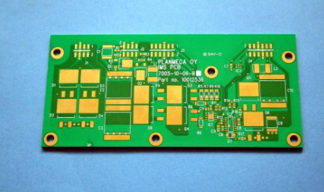
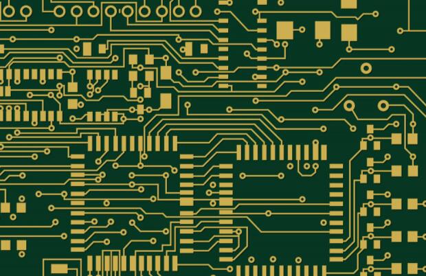
Factors affecting the quality of exposure imaging by circuit board factories
The process technology in the circuit board production process is possible if the editor of the circuit board manufacturer talks for three days and nights and the previous part is possible. Our staff strictly control every production detail of the circuit board factory, and we still give it today. We share those factors that affect the exposure and imaging of the circuit board factory. Those who are interested must come and have a look. We have our own freestyle belonging to our circuit board factory (PCB circuit board manufacturer).
Factors affecting the quality of exposure and imaging by the circuit board factory:
One, the choice of light source
In the circuit board factory (Shenzhen PCB circuit board manufacturer), any kind of dry film has its own unique spectral absorption curve, and any kind of light source also has its own emission spectrum curve. If the main spectral absorption peak of a certain dry film overlaps or most overlaps with the main spectral emission peak of a certain light source, the two match well and the exposure effect is the best. The spectral absorption curve of domestic dry film shows that the spectral absorption region is 310~440nm. Dysprosium lamp, high pressure mercury lamp, and iodine gallium lamp have relatively large relative radiation intensity in the wavelength range of 310~440nml, which is an ideal light source for dry film exposure. .

2. Exposure time control
In the light-gathering process, the photopolymerization reaction of the dry film does not complete the reaction at the sight of light, but requires a certain exposure time
make an adequate response:
When the exposure is insufficient, due to the incomplete polymerization of the monomer, the film swells and becomes soft during the development process, and the lines are not clear.
The color is dim, or even stale. During the pre-treatment of electroplating or the process of electric quilting, the film is warped, infiltrated, or even peeled off;
In the circuit board factory (Shenzhen PCB circuit board manufacturer), it will be difficult to develop, the film will be brittle, and residual glue will be left when overexposure; incorrect exposure will cause deviation of image line width, and excessive exposure will Make the lines of the pattern plating thinner, and make the printed and etched lines thicker. On the contrary, insufficient exposure makes the pattern plating lines thicker and the printed and etched lines thinner. In order to determine the exposure time, it is usually recommended to use a Riston 17-level or Sbuffer 21-level optical densitometer.
The circuit board factory (Shenzhen PCB circuit board manufacturer) also needs to pay attention to the visual positioning in the exposure positioning:
The visual positioning of the circuit board factory is usually suitable for the use of a diazo master. The diazo master is brown or orange in a semi-transparent state; but it is not transparent to ultraviolet light, and the pad of the master is overlapped with the hole of the printed board through the diazo image. Align and fix with tape to perform exposure.
The above is the freestyle of the small circuit board factory. I don't know if you already understand it. These are the factors that affect the quality of exposure and imaging of the circuit board factory.
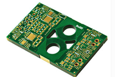
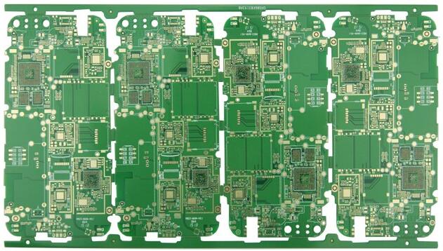
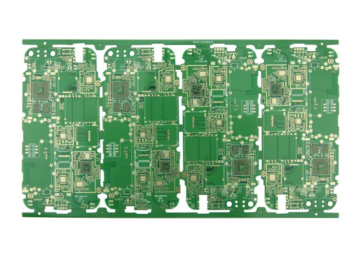
iPCB is a high-tech manufacturing enterprise focusing on the development and production of high-precision PCBs. iPCB is happy to be your business partner. Our business goal is to become the most professional prototyping PCB manufacturer in the world. Mainly focus on microwave high frequency PCB, high frequency mixed pressure, ultra-high multi-layer IC testing, from 1+ to 6+ HDI, Anylayer HDI, IC Substrate, IC test board, rigid flexible PCB, ordinary multi-layer FR4 PCB, etc. Products are widely used in industry 4.0, communications, industrial control, digital, power, computers, automobiles, medical, aerospace, instrumentation, Internet of Things and other fields.