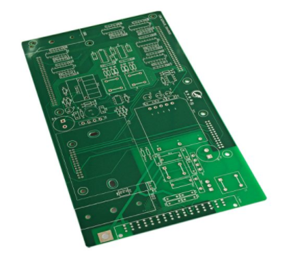
How to reduce ripple generation in PCB design? Negligence in PCB design of switching power supply can paralyze the entire circuit due to ripples in the power network. If not detected, power ripple can cause serious signal integrity problems.
What causes power ripple
Power ripple is a phenomenon caused by the switching characteristics of power supply. It usually occurs in switching power supplies, where inductance and capacitance introduce noise caused by switching frequency. The power ripple introduced by the switching frequency usually resonates at low frequencies.
However, low-frequency power ripple is not a concern for PCB designers. High-frequency power ripple or ringing can also be introduced into the output of the switching power supply by the parasitic capacitance of the inductor. Ringing occurs during the on-off transition of the switching power supply and is identified by spikes along the ripple.

How do power ripples affect electronic circuits
The boat cruised through the soft waves without problem. But electronic circuits that rely on clean power cannot say the same. At both low and high frequencies, power ripple may impair circuit function.
Ripples in voltage wiring may cause crosstalk with adjacent circuits. High-frequency ringing on the power line will be coupled to signal pins on the IC. It is true that most ics can tolerate a certain amount of noise, but noise at higher frequencies exceeds the power rejection ratio.
When switching mode noise and ringing start to be coupled to the signal, it compromises the accuracy of the input reading. Communication signals and power ripple can cause signal integrity problems. Power ripple is more than just a nuisance. This is a serious problem that can paralyze electronic circuits.
How to reduce power ripple in PCB design
Unless you are designing a PCB with a linear power supply, you will have to deal with power ripple. To reduce the effect of the power ripple, you must reduce the amplitude of the initial peak and subsequent ripple.
Here are some handy tricks to solve power ripple in design.
1. Buffer circuit
A buffer circuit consisting of a resistor and capacitor can be placed at both ends of the switch node of a low-end mosfet in a switching power supply to reduce ringing. Both RC combinations act as dampers, absorbing the energy released when the mosfet changes state. The use of buffer circuits helps to reduce EMI emitted by ringing.
2. Guide resistance
The bootstrap resistance limits the initial branch of ringing noise. It is placed at both ends of a high-end MOSFET gate in series with a bootstrap capacitor. When starting resistors are added to the PCB design, the charging time of the mosrfet is increased to suppress the initial peak. You need to be careful about the value of the starting resistance, because too little current can affect the performance of the SWITCHING power supply. Ripple can be reduced by limiting the charging current of the mosfet.
3. Heart-piercing capacitance
You might think it would be a good idea to use capacitors to eliminate ripples. But typical capacitors only help to filter out low frequency noise. In order to reduce high-frequency ripple, try to use the current capacitor. The core capacitor has three terminals to produce better insertion loss at high frequencies.
Of course, it is important to believe that a reliable simulation tool that can accurately model power supplies and power ripple through a vast library of new model parameters will greatly improve your chances of designing a circuit that power ripple cannot overcome.
In general, all of the above methods are used simultaneously to provide better performance for switching power supplies. As a PCB designer, you will want to minimize power ripple without compromising power efficiency.