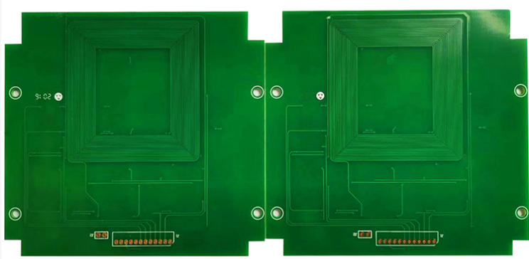
What is a characteristic impedance PCB board?
Characteristic impedance refers to the resistance of the high-frequency signal or electromagnetic wave in the propagation process of the transmission signal line relative to a certain reference layer at a certain frequency, which is also called characteristic impedance. It is equivalent to a vector sum of electrical impedance, inductive reactance, and capacitive reactance. (Characteristic impedance PCB board)
What's the point of making characteristic impedance PCB board?
Characteristic impedance is the core of solving signal integrity problems.
With the continuous development of PCB electronic products towards high frequency and high speed, the circuit performance provided by PCB must ensure that the signal does not reflect during the transmission process and keep the signal intact and undistorted.

In order to ensure signal integrity, the characteristic impedance (Z0) of the signal line of the PCB must be matched with the "electronic impedance" of the head and tail components; when electronic devices such as computers and communication switches are in operation, the signals sent by the drive components need to pass through the PCB The signal line reaches the receiving element.
Impedance-actually refers to the parameters of resistance and reactance, because the PCB circuit (board bottom) should consider plugging and installing electronic components, and the conductivity and signal transmission performance should be considered after plugging. Therefore, the lower the impedance, the better. The resistivity should be lower than the minus 6th power of 1*10 per square centimeter.
The characteristic impedance PCB board under the normal design components, affect the relationship of the impedance related factors:
1. The thicker the dielectric layer, the greater the impedance value;
2. The larger the dielectric constant, the smaller the impedance value;
3. The thicker the copper foil, the smaller the impedance value;
4. The larger the line width, the smaller the impedance value;
5. The thicker the ink thickness, the smaller the resistance value.
The above is the introduction to the knowledge of characteristic impedance PCB board, I hope it will be helpful to you!
iPCB is a high-tech manufacturing enterprise focusing on the development and production of high-precision PCBs. iPCB is happy to be your business partner. Our business goal is to become the most professional prototyping PCB manufacturer in the world. Mainly focus on microwave high frequency PCB, high frequency mixed pressure, ultra-high multi-layer IC testing, from 1+ to 6+ HDI, Anylayer HDI, IC Substrate, IC test board, rigid flexible PCB, ordinary multi-layer FR4 PCB, etc. Products are widely used in industry 4.0, communications, industrial control, digital, power, computers, automobiles, medical, aerospace, instrumentation, Internet of Things and other fields.