The mysterious copper substrate finally reveals its true face
Circuit board factory: Copper substrate is the most expensive kind of metal substrate, and its thermal conductivity is many times better than aluminum substrate and iron substrate. It is suitable for high-frequency circuits and areas with large changes in high and low temperature, as well as heat dissipation and architectural decoration of precision communication equipment. industry.
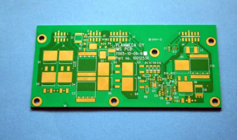
Copper substrates are divided into gold-immersed copper substrates,silver-plated copper substrates, tin-sprayed copper substrates, and oxidation-resistant copper substrates.
The circuit layer of the copper substrate is required to have a large current-carrying capacity, so thicker copper foil should be used, the thickness is generally 35μm~280μm;
The thermal insulation layer is the core technology of the copper substrate. The core thermal component is composed of aluminum oxide and silicon powder and epoxy resin filled polymer. It has low thermal resistance (0.15), excellent viscoelasticity, and thermal aging resistance. Ability to withstand mechanical and thermal stress.
The metal base layer is the supporting member of the copper substrate, which requires high thermal conductivity, and is generally a copper plate, which is suitable for conventional machining such as drilling, punching and cutting.

The basic production process of copper substrate:
1. Cutting: Cut the raw material of the copper substrate into the size required in the production.
2. Drilling: Positioning and drilling of copper substrate plates will provide help for subsequent processing.
3. Circuit imaging: present the required part of the circuit on the copper substrate sheet.
4. Etching: Keep the required parts after the circuit is imaged. The rest does not need to be partially etched away.
5. Screen printing solder mask: prevent non-soldering points from being contaminated with solder and prevent tin from entering and causing short circuits. The solder mask is particularly important when performing wave soldering, which can effectively protect the circuit from moisture.
6. Silk screen characters: for marking.
7. Surface treatment: protect the surface of the copper substrate.
8. CNC: Perform numerical control operations on the entire board.
9. Withstand voltage test: test whether the circuit is working normally.
10. Packaging and shipping: The copper substrate confirms that the packaging is complete and beautiful, and the quantity is correct.
In PCB proofing, copper substrates are special boards. In addition to being expensive, they also have certain technical thresholds and difficulty in operation. Some PCB manufacturers find it troublesome or think that the number of customers' orders is small, so they don't want to do it or do less.