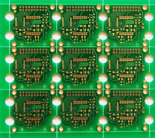
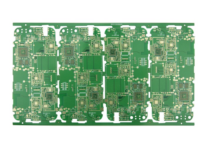
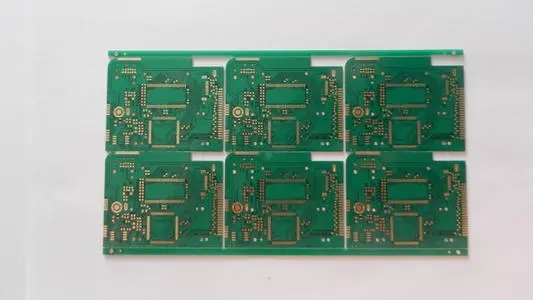
PCBA board distortions occur in PCBA batch production in PCBA board manufacturer. PCB board distortions will have a considerable impact on patches and testing. Therefore, this problem should be avoided in PCBA processing production.
Technical engineers at IPCB in Shenzhen analyzed several causes of PCBA distortion:
1. Inappropriate selection of PCB raw materials, such as low T value of PCB, especially paper-based PCB, will cause PCB to bend because of its high processing temperature.
2. Improper PCB circuit board design, uneven distribution of components will not cause excessive PCB thermal stress, larger connectors and sockets will also affect the expansion and contraction of PCB circuit board, which will lead to permanent distortion of PCB circuit board;
3. PCB circuit board design problems, such as double-sided PCB circuit board, if one side of the copper foil is retained too large, such as ground wire, and the other side of the copper foil is too small, this will also cause uneven contraction of both sides and PCB distortion.
4. The clamp used improperly in PCBA processing or the clamp distance is too small, for example, the clamp of finger claw is too tight during peak welding, PCB will expand and appear PCB distortion due to the welding temperature;

5. High temperature in reflow soldering may also cause distortion of PCB.
For the above reasons, the PCBA engineers of Shenzhen IPCB proposed corresponding solutions based on their rich experience:
(1) Choose PCB with high Tg or increase PCB thickness to obtain the best aspect ratio when the price and space of PCB circuit board allow;
(2) The technical engineer of PCBA board manufacturer needs to design PCB rationally. The area of double-sided steel foil should be balanced. Copper layer should be covered in place without circuit and appear as grid to increase the hardness of PCB.
(3) Operators of the patch processing plant pre-bake the PCB before the PCBA patch, provided that it reaches the standard of 125 C/4h;
(4) Smt technicians adjust the clamp or clamp distance before PCBA processing to ensure the space for PCB to expand under heat;
(5) The welding process temperature should be lowered as much as possible during PCBA processing. If the PCBA circuit board has been slightly distorted, it can be placed in the fixture and reset to release the stress. Generally, such a treatment will also achieve satisfactory PCBA quality results.