Trend Analysis of Global Top 100 PCB Companies
Recently, according to CPCA Printed Circuit Information, the global PCB (printed circuit board) top 100 companies in 2019 are the overall situation trend analysis:
The proportion of selected domestic enterprises in China has continued to rise sharply since 2001 (it has remained stable in the past two years). Decades ago, it surpassed Japan to become the world's largest producer of printed circuit boards, with both output and output value ranking in the forefront. The current products are mainly concentrated in single and double-sided rigid boards, multilayer boards, FPCB, HDI, and high-level digital boards.
my country's PCB is so good and you don't know it? I guess you know the existence of PCB and know what it does. But you don't know what it is? Then look down, you will definitely realize it!
1. What is a printed circuit board?

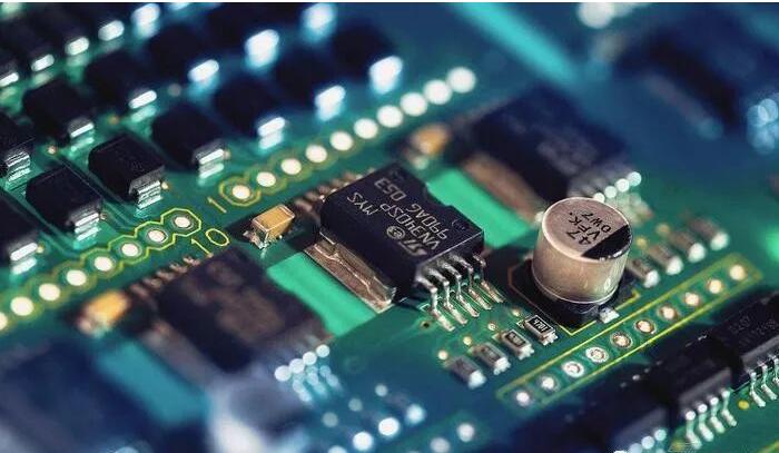
Printed circuit boards (PCB) for short; also called printed circuit boards, circuit boards; it is the provider of electrical connections for electronic components, mainly for transmission and conduction. It is the substrate for assembling electronic components (mainly composed of two types of materials: insulating base material and conductor), the kind without any components on it; the final IC board composed of complete components is different from the circuit board; To put it bluntly, it is the base of the IC integrated circuit.
2. Composition structure and process:
The printing structure is relatively simple, mainly composed of lines and graphics, dielectric layers, vias, solder mask, surface treatment and bare boards, etc.;
Circuit and surface: The circuit is used as a tool for conduction between the originals. In the design, a large copper surface will be additionally designed as a grounding and power layer. The route and the drawing are made at the same time.
Dielectric layer (Dielectric): used to maintain the insulating substrate between the circuit and each layer.
Hole (Through hole / via): The through hole can make the lines of more than two levels connect to each other, the larger through hole is used as a part plug-in, and there are non-through holes (nPTH) usually used as surface mount For positioning and fixing screws during assembly.
Solder resistant /Solder Mask: Solder resistant /Solder Mask printed in the non-tin-eating area to isolate the copper surface from the tin-eating substance (usually epoxy resin), to avoid short circuits between the non-tin-eating lines, according to different processes, Divided into green oil, red oil and blue oil.
Silk screen (Legend /Marking/Silk screen): Mark the name and position frame of each part on the circuit board to facilitate maintenance and identification after assembly.
Surface Finish: Since the copper surface is easily oxidized in the general environment, it can not be tinned (poor soldering properties), so it will be protected on the copper surface that needs to be tinned. The protection methods include HASL, ENIG, Immersion Silver, Immersion Tin, and Organic Solder Preservative (OSP). Each method has its advantages and disadvantages, which are collectively referred to as surface treatment.
3. The production process of printed circuit:
As a bridge that carries electronic components and connects circuits, PCB is an indispensable key basic component in the electronic information industry. Because it is made by electronic printing, it is called a "printed" circuit board. The PCB production process of the printed circuit board is as follows:
Fourth, the type of printed circuit board
Printed circuit boards are mainly divided into three major categories: single-sided board, double-sided board, and multi-layer circuit board;
1. Single-sided board. On the most basic PCB, the parts are concentrated on one side, and the wires are concentrated on the other side. Single-sided panels are usually simple to manufacture and low in cost, but the disadvantage is that they cannot be applied to products that are too complex.
2. Double-sided board is an extension of single-sided board. When single-layer wiring cannot meet the needs of electronic products, double-sided board should be used. There are copper-clad wires on both sides, and the lines between the two layers can be connected through vias to form the required network connections.
3. Multi-layer boards are used to meet more complex application requirements. Circuits are arranged in a multi-layer structure and pressed together, and through-hole circuits are arranged between layers to connect the circuits of each layer. Multilayer boards have the advantages of high assembly density, small size and light weight;
Seeing this, do you already understand what the PCB is? 90% of communication equipment and electronic equipment in life have its traces, and where there are integrated circuits, they exist! Would you like to take a look at your earphones, mobile phone, and charger?